In the last two posts, we covered quite a bit of the von Neumann architecture and how The 4043 breadboard computer maps to it. This is the third post in a 3-part series on computer architecture and how I built an 8Bit breadboard computer inspired by Ben Eater. If you haven’t read posts one and two, go read them first.
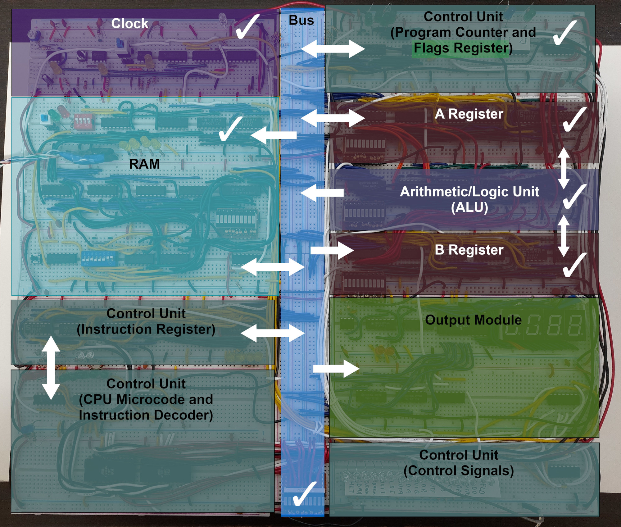
In this post, we will be concluding the series. We will discuss the output module (highlighted in green) and the control logic for the computer (everything else that isn’t ticked, and the Flags Register which we skipped last time). Let’s get started!
Refresher
A quick refresher, we talked in the first post about the “bare minimum” computer which needs:
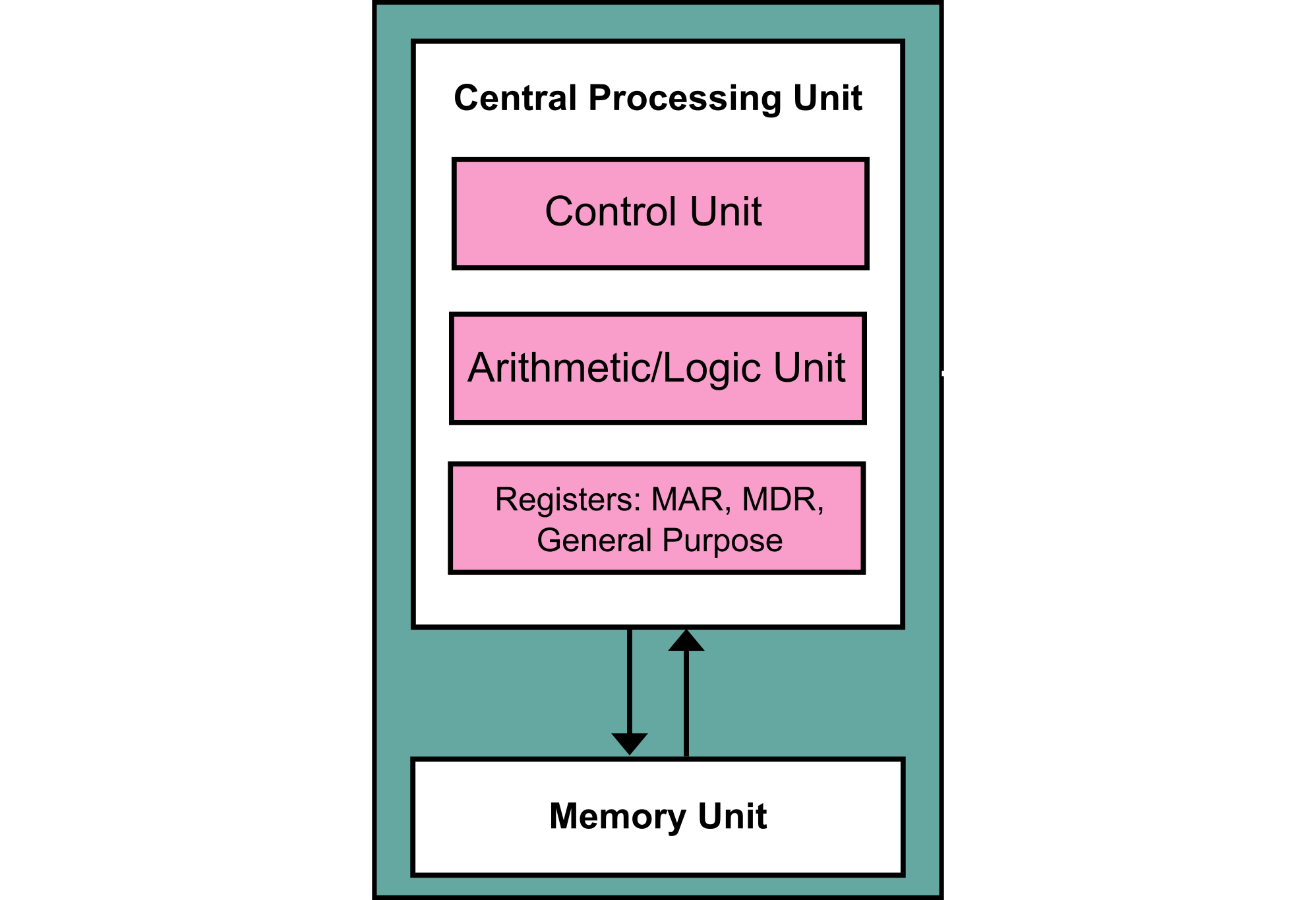
- CPU:
- Registers (✓)
- ALU (✓)
- Control Unit (—)
- RAM (✓)
- Bus to connect them together (✓)
- Clock to sync all of these components together (✓)
Key:
- ✓ - Discussed
- — - Still To be Discussed
By now, we have an idea of how all of these modules work on their own and how they work with each other. What controls them, though? How does a register know when to load a value? When would RAM output a value it is storing at a certain address? We will get into these topics in this post. First, I want to talk about one last module that was built before the control logic: The output module.
Input/Output
I/O is part of the von Neumann architecture, and that makes sense as a computer won’t be all that useful without some form of input and output. By I/O here, we don’t just mean user input and output such as keyboards, mice, speakers, and monitors. We mean any device that communicates with the CPU of the computer and vice versa. This includes Ethernet controllers, storage device controllers, GPUs, and pretty much anything that the CPU communicates with.
I/O is usually done through ports, ports are basically an interface between a computer and any other device. This device can be part of your personal computer overall, but not part of the “bare minimum” computer we’ve been talking about. For example, your computer will function without a storage device controller, but I bet you won’t be able to do much work without a functioning OS which requires some form of storage device to be loaded from.
The summary here is that all devices, even “internal” ones, communicate with the CPU through an I/O port. Modern CPUs mostly have this “port” as a memory location (in the case of memory-mapped I/O) or an actual port from a separate address space (in the case of port-based I/O). This is a bit of a big topic, so I won’t get into it.
Modern computers use chipsets on the motherboard and a lot of other devices to help the CPU communicate with all these devices, we won’t get into that but it is generally a nice topic to look up.
I/O in The 4043
In our breadboard computer, we have only one output device and no input devices. The output device is a seven-segment display module which can be used to display whatever is in the A register. As for input, we don’t have any interactive user input. The user can only interact with the computer via programming it through the memory module. i.e. manually placing the opcodes for instructions and data in memory.
We are communicating with the output module using the bus, and the device has a load signal which allows it to read what is on the bus and display it. This may sound simple, but it becomes really troublesome if we want to add other I/O devices. As each device would need its control pins hard-wired to the CPU. This is a limitation in our breadboard computer’s design, but it really isn’t that hard to implement more I/O devices. We’d just have to add more microcode(explained later) and connections to handle these instructions.
This is why typically CPUs use a separate chip for I/O which can be used to address and communicate with different devices. An example of such a chip is the Intel 8255 chip which was commonly used with the original Intel 8086 processor.
At the end of this post, I have added a link to a Reddit post where someone added more I/O and parts to the computer and was able to get the 8Bit breadboard computer to run the game Snake.
Now we have an idea of everything we need to know in order to start talking about the control unit.
The Control Unit
The control unit is the actual “manager” of the CPU, in the sense that it tells each module when and what to do so that each instruction is executed properly. In order to understand how the control unit operates, we need to differentiate between three things: a clock cycle, an instruction cycle, and a micro-instruction.
Clock Cycle
A clock cycle is a single pulse of the clock signal. i.e. a single transition from 0V to 5V and then back to 0V again.
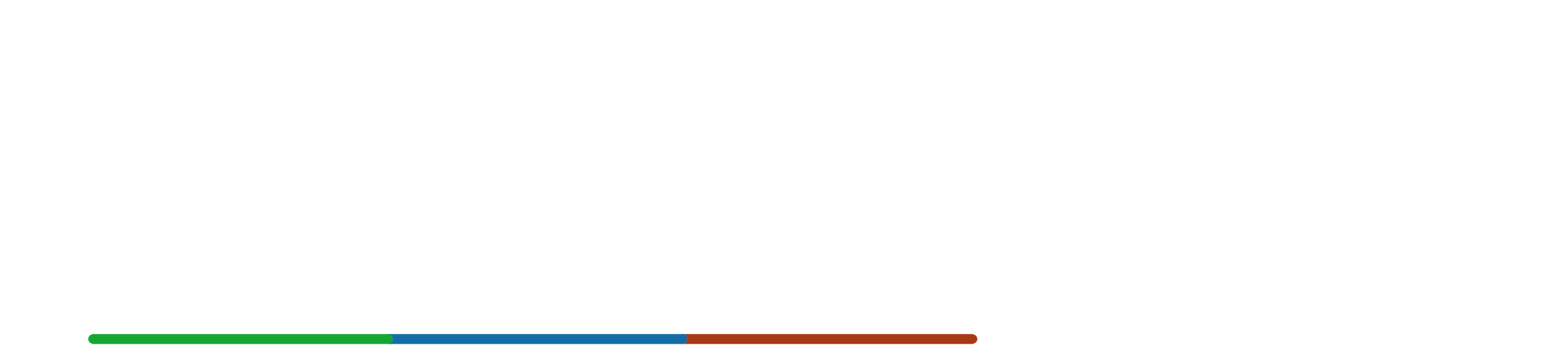
Each coloured section here is a single clock pulse
Instruction Cycle
Every single CPU has an instruction cycle. This cycle is different between different architectures. But, generally, it follows something like the following figure.
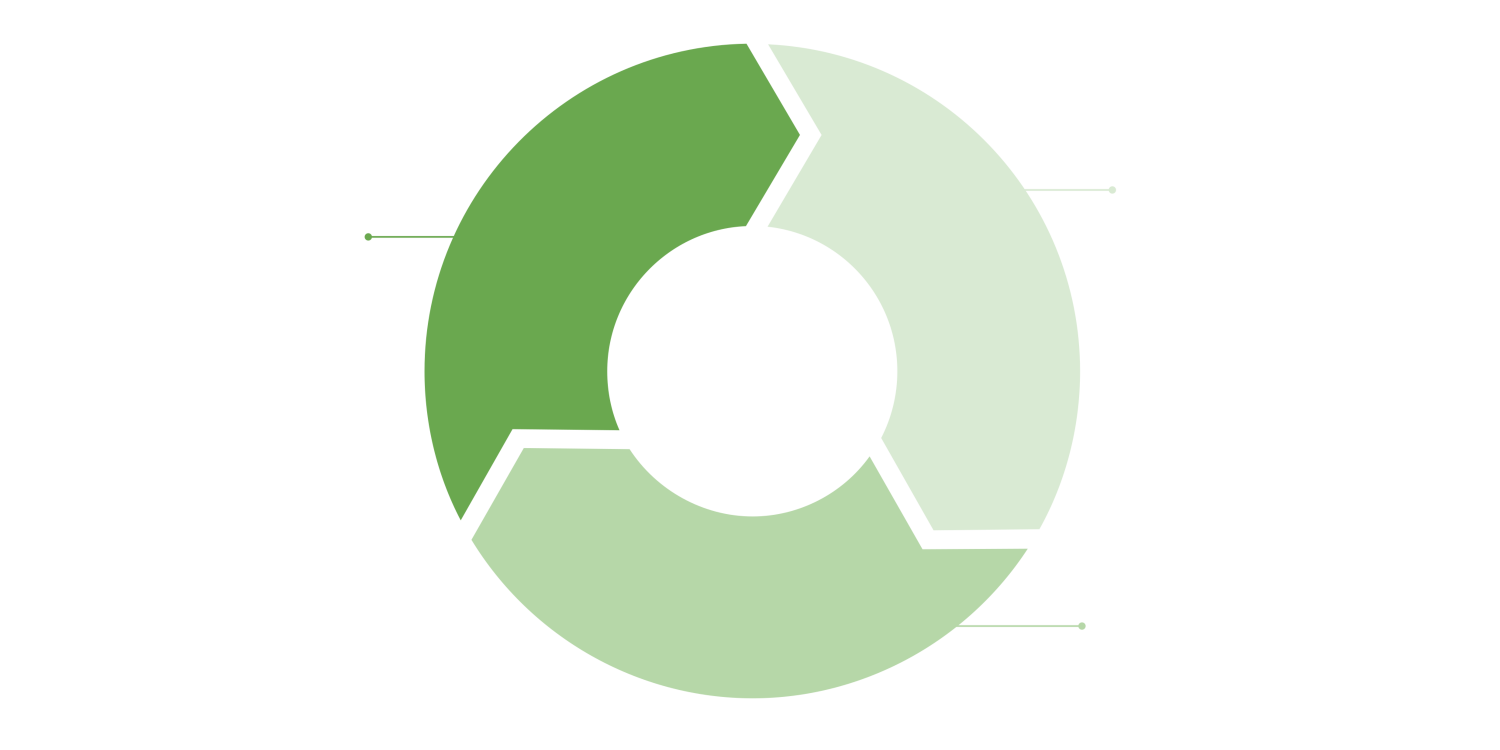
- The instruction is fetched from memory. If you remember, in the last post we touched on how the program counter is used to determine which address from memory the due instruction will be fetched from
- The instruction is decoded by the control unit. This is the stage where the control unit understands what the instruction will do. Based on the instruction, the control unit sends control signals to prepare the instruction for execution. For example, it would fetch any required data from memory
- The instruction is finally executed. The control unit sends control signals to all modules that are relevant to this execution. For example: If the instruction was going to subtract, it would send a subtract (
SUB) signal to the ALU - This cycle is repeated for as long as the computer hasn’t been turned off or halted for any reason
Every single instruction ever executed on a computer follows an instruction cycle similar to this. Even the popular nop instruction which stands for “No Operation”, still gets to the “Execute” phase and the control unit would then let the components be idle until the current instruction cycle finishes execution.
A little bit of trivia, in the x86 architecture(before 64-bit iterations): nop (opcode 0x90) was actually just an alias for xchg eax, eax which basically swaps the value in the eax register itself, to end up doing literally nothing.
Micro-Instructions
A micro-instruction is what each instruction divides into. Each instruction is basically a set of actions the computer needs to do. Each action is considered a micro-instruction.
Now, is it safe to assume that each instruction cycle takes 3 clock cycles? No. Each instruction cycle consists of several micro-instructions. In our breadboard computer, we have a max of 8 micro-instructions per instruction. However, actual instructions that are implemented can take anywhere from 2 to 5 micro-instructions. We will get to know why it requires a minimum of 2 in a bit. Each micro-instruction takes one clock cycle.
Micro-instructions are usually labelled as Tn Let’s take a look at an example: Say you want to move a value to the A register, the computer would have to do the following micro-instructions:
The Fetch Phase:
- T1: Move the content of the program counter into the memory address register
- This is to address the instruction that is to be executed, which is kept track of using the program counter
- At this point, the memory data register already loaded the value at the memory address since it reads the address from the MAR automatically
The Decode Phase:
- T2: The MDR is set to output its content, the Instruction register is set to load what’s on the bus, and the program counter is incremented
- Once the Instruction register has loaded the value in memory (the instruction), it is automatically decoded by the control unit and the execution phase is prepared
The Execution Phase:
- T3: The value is output from the instruction register onto the bus and the A register is set to load what’s on the bus
- T4: The computer does nothing
- T5: The computer does nothing
- Step 6(actually back to T1): Rinse and repeat!
Now to answer the question, why does each instruction need at least 2 micro-instructions? We need one for fetching and one for decoding. Depending on what was decoded, we may or may not need more micro-instructions for the execution phase.
The Control Word
But, now you’re probably wondering: “What is a micro-instruction actually doing?” How does it tell the A register to load what’s on the bus or tell the program counter to count?
The answer is simply through control signals, which the control word consists of.
Control Signals
The control word consists of 17 signals. 16 of which are relevant to our microcode. Our computer never uses the OUTB signal (which outputs whatever is in the B register to the bus), I just added it for completeness. Thankfully, it sits right in the middle between the high 8 signals and low 8 signals so we can consider it a divider.
Each signal can have two values: high or low. When a signal is high it functions, effectively signalling the module what to do.
| Signal | Description | Signal | Description |
|---|---|---|---|
HLT |
Halt Execution | LDB |
Load what’s on the bus into the B reg. |
LDMA |
Load what’s on the bus into the MAR | OUTΣ |
Output the ALU’s output to the bus |
OUTMEM |
Output what’s in the MDR onto the bus | SUB |
Set the ALU to subtract instead of add |
LDMEM |
Load what’s on the bus into the MDR | PCC |
Make the PC count |
OUTI |
Output what’s in the IR onto the bus | LDPC |
Load what’s on the bus into the PC |
LDI |
Load what’s on the bus into the IR | OUTPC |
Output what’s in the PC onto the bus |
OUTA |
Output what’s in the A reg. onto the bus | LDO |
Load what’s on the bus into the Output |
LDA |
Load what’s on the bus into the A reg. | FLD |
Load the state of the Flags Reg. |
To sum it up, each instruction consists of micro-instructions, and these micro-instructions consist of control signals that are enabled/disabled based on what the computer needs to do. This is exactly how our computer works(and most other computers do).
We will visualise this in a bit and trace a program written in 4043 assembly.
Implementing the jmp
I remember asking you to think of a way to implement a jmp instruction. Have you thought of one?
Well, now that we know the control signals for the computer, we can actually use the LDPC and depending on our architecture, output the value of some register or memory location to the bus to load it in the program counter. This effectively makes the CPU fetch the next instruction from the address that was loaded into the program counter, making it the next instruction to be executed.
The 4043 Assembly
Our computer has a limited set of simple instructions. Limited they are, but the computer is still Turing complete and can compute pretty much anything. Although we have two major limitations which are its speed and the size of the RAM being only 16 bytes. Some people even argue that this computer isn’t really an 8Bit computer since it isn’t able to address 256 bytes of memory and can’t have an instruction set of more than 16. I think it’ll do for now regardless of that.
| Instruction | Opcode | Description | Summary |
|---|---|---|---|
nop |
0000 |
No Operation | |
lda addr |
0001 |
Load value in addr in memory into the A register | A = [addr] |
add addr |
0010 |
Add value in addr in memory into the A register | A += [addr] |
sub addr |
0011 |
Subtract value in addr from the A register | A -= [addr] |
sta addr |
0100 |
Store the value in the A register in addr in memory | [addr] = A |
ldi imm |
0101 |
Loads the value imm to the A register | A = imm |
jmp addr |
0110 |
Jumps to addr, i.e. sets the program counter to addr | PC = addr |
jc addr |
0111 |
Same as jmp, but if the Carry Flag (CF) is set (high) |
|
jz addr |
1000 |
Same as jz, but for the Zero Flag (ZF) |
|
out |
1110 |
Outputs the content of the A register on the 7-segment display | |
hlt |
1111 |
Halts execution |
But, how does the CPU map which instructions use which micro-instructions on which cycle?
CPU Microcode
For each instruction, we have five micro-instructions. We have a counter that counts from 0 to 4 for each instruction, thus allowing the computer to know which micro-instruction it is executing. Depending on which micro-instruction we’re on and the instruction loaded, these values are used to address into an EEPROM. The EEPROM stores values that represent the signals we mentioned before.
For example, we can program the EEPROMS with values such as the following to implement instructions.
microcode[16][8] = {
   //T1         //T2            //T3         //T4     //T5           //T6 - T8, not used
  {LDMA|OUTPC,  OUTMEM|LDI|PCC,  0,          0,           0,             0, 0, 0},   // 0000 - NOP
  {LDMA|OUTPC,  OUTMEM|LDI|PCC,  OUTI|LDMA,  OUTMEM|LDA,  0,             0, 0, 0},   // 0001 - LDA
  {LDMA|OUTPC,  OUTMEM|LDI|PCC,  OUTI|LDMA,  OUTMEM|LDB,  OUTS|LDA|FLD,  0, 0, 0},   // 0010 - ADD
  ... //More instructions, check GitHub
You can see the full microcode on Ben Eater’s GitHub.
Summary is:
Micro-Instruction + Instruction's opcode = Address
Address into EEPROM + state of the Flags Register = control signal values
Your First 4043 Program
Let’s write a small 4043 program! How about a program that keeps adding 5 to the A register, outputs the result on the seven-segment display, and then halts execution once it goes past 255 (overflows)?
The program is pretty simple, but it effectively uses almost 40% of our available memory. This really shows the limitation of The 4043.
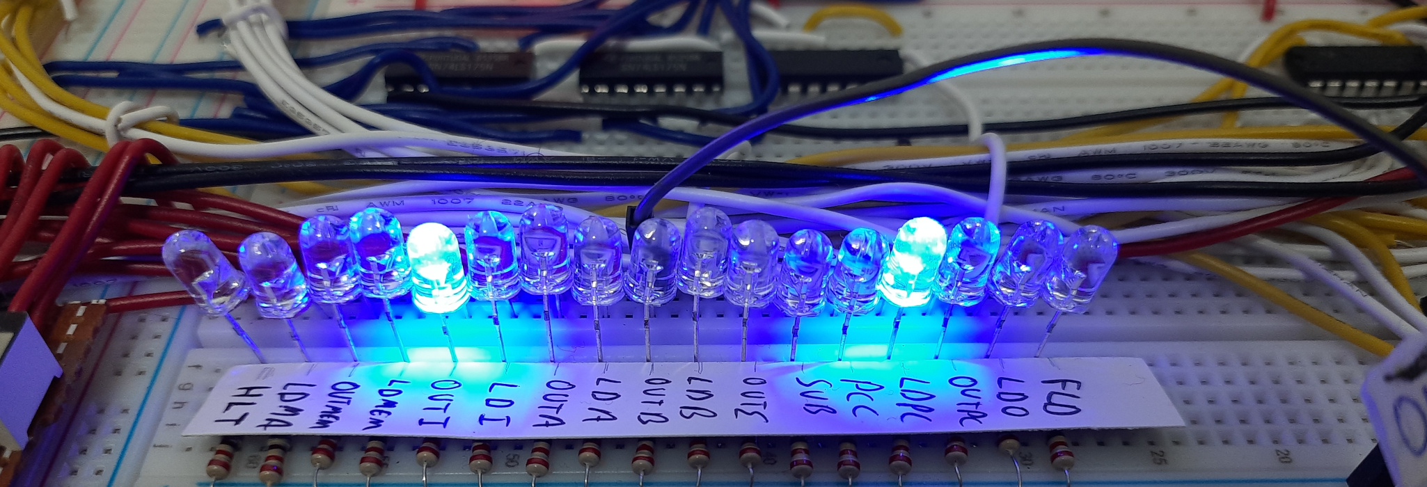
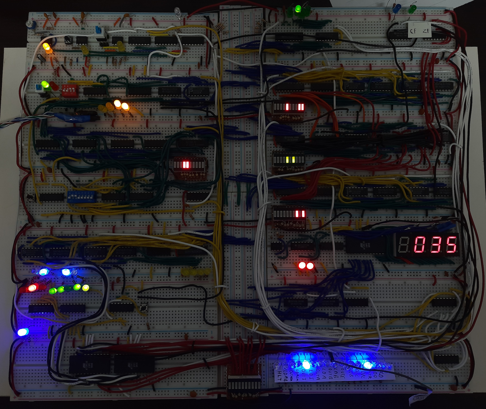
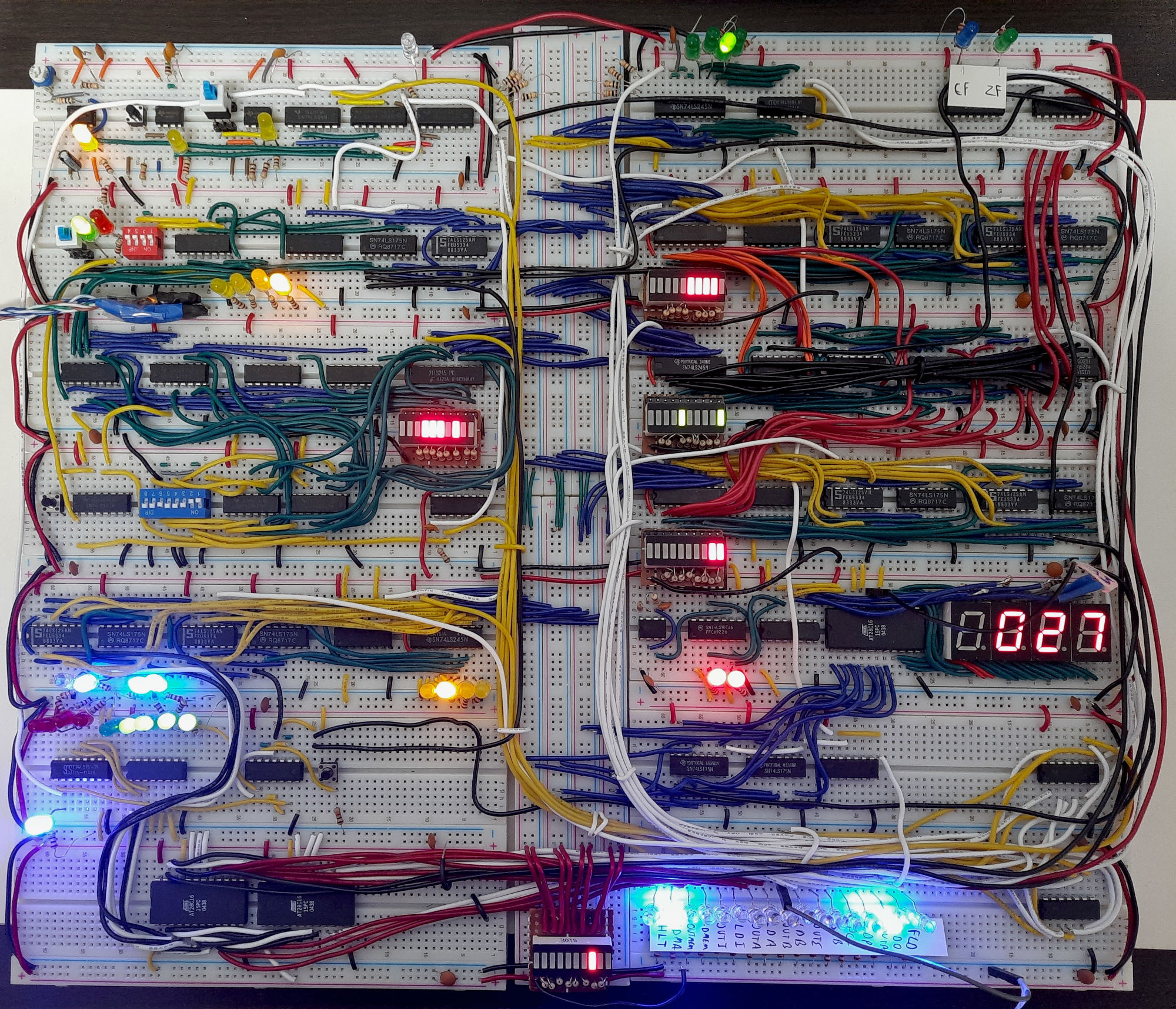
The state of the computer after this program finishes executing, notice the HLT signal
Let’s trace what happens in each micro-instruction!
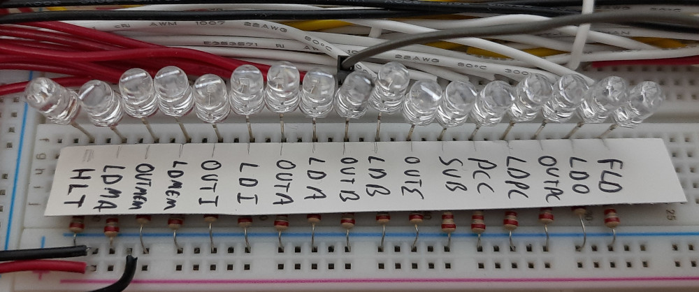
In the following animations, the LEDs at the bottom left indicate which micro-instruction we’re executing. Each component of the computer has its control lines connected to the Control Unit. Look at the changes between each of the diagrams and it should map to what we discussed earlier.
add 5
This instruction in binary is 0010 (add), 0101 (5), making it 00100101.
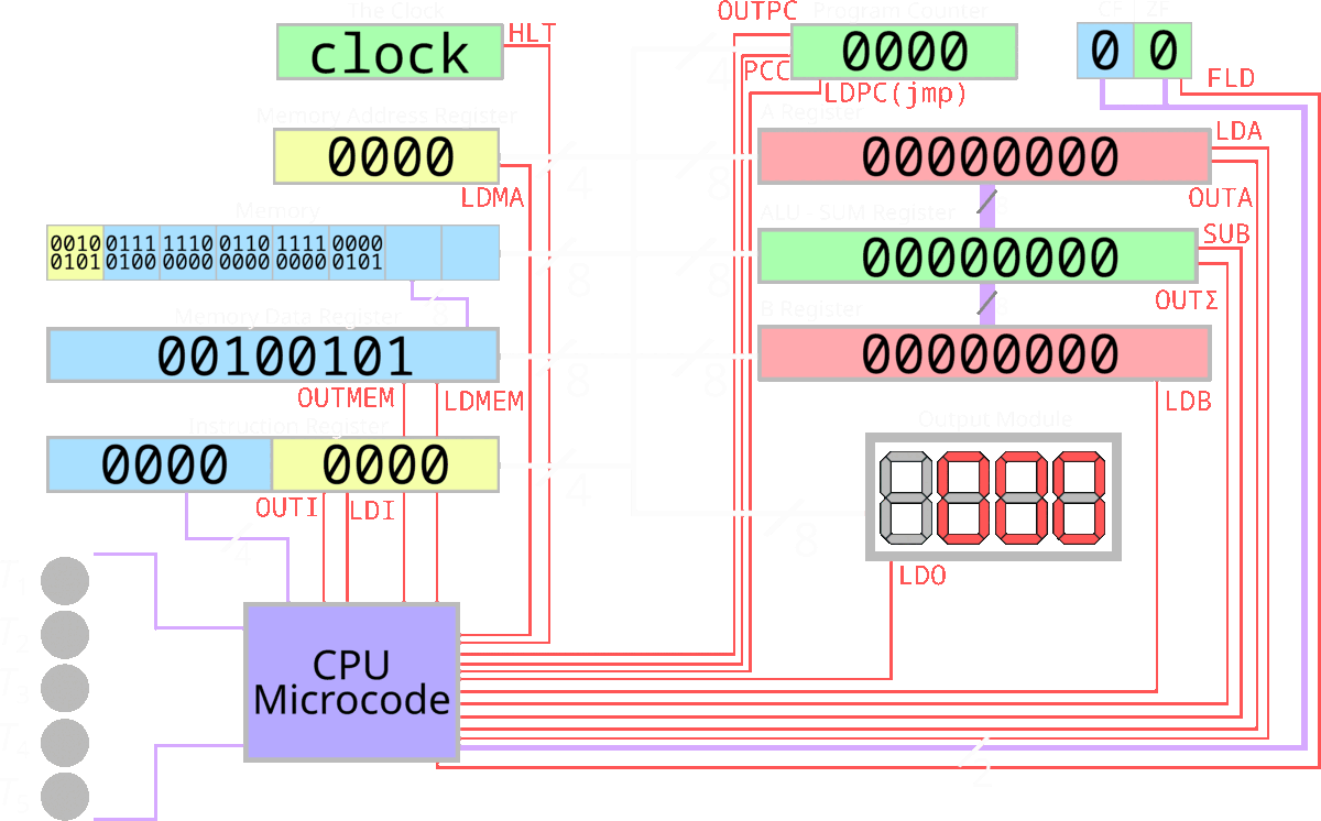
We can see that in each micro-instruction, the control unit is enabling components based on the CPU microcode. The signals are determined through a combination of the micro-instruction counter, the opcode coming from the Instruction register, and the values in the flags register. Let’s take a look at two more instructions before we talk about one final thing and then wrap up this really long post.
We still skip looking at jc 4 because it isn’t really that different from a jmp. The only difference is that jc will only work if the Carry flag is set. Look at the jmp 0 section and from there, you should be able to figure out how jc works.
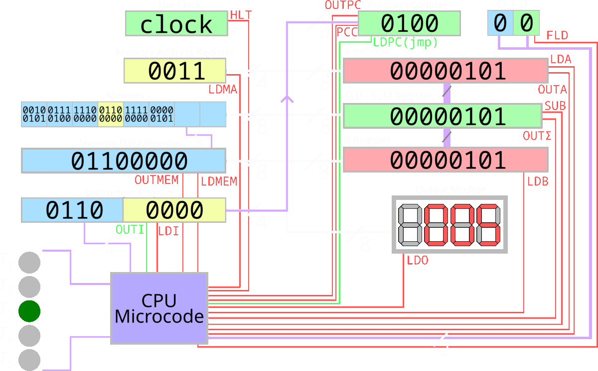
out
For this instruction, we will skip T1 and T2 as they are the same for every instruction. All we’re going to look at is T3 to T5. As of the start of T3, the instruction has been fetched and is now in the instruction register and the program counter has been incremented.
This instruction in binary is 1110 (out) and the rest of the bits don’t really matter but I like to set them to 0 when programming the computer, making it 11100000.
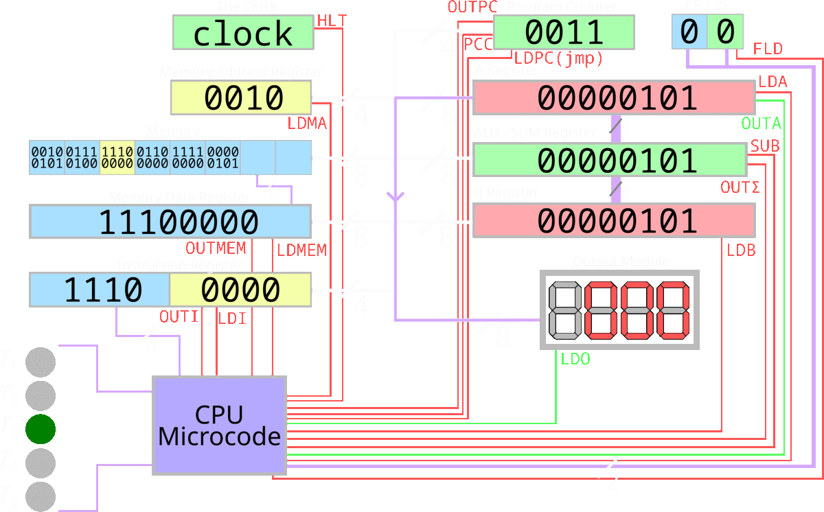
In this instruction, after T3, the control unit isn’t doing anything interesting. It already set the control lines at T3 and the only remaining thing was the clock to pulse. That’s why at T4 we see the output module’s display change to a 5.
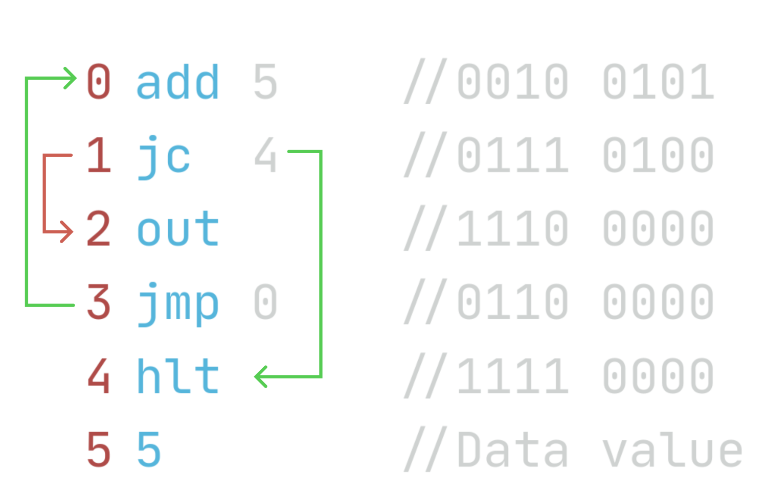
jmp 0
For this instruction, we will also be skipping T1 and T2 as they are the same for every instruction. This instruction in binary is 0110 (jmp), 0000 (0), making it 01100000.
As we can see all this unconditional jmp does is load the specific address (0) in the program counter. We can see that T1 and T2 of the next instruction are basically fetching and decoding add 5 which, indeed, is the instruction at address 0.
A picture of the jmp instruction, notice the OUTI and LDPC signals
The Build
On days 8, 9, and 10, I built the EEPROM programmer, the output module, and the control unit.
Module 6: The EEPROM Programmer
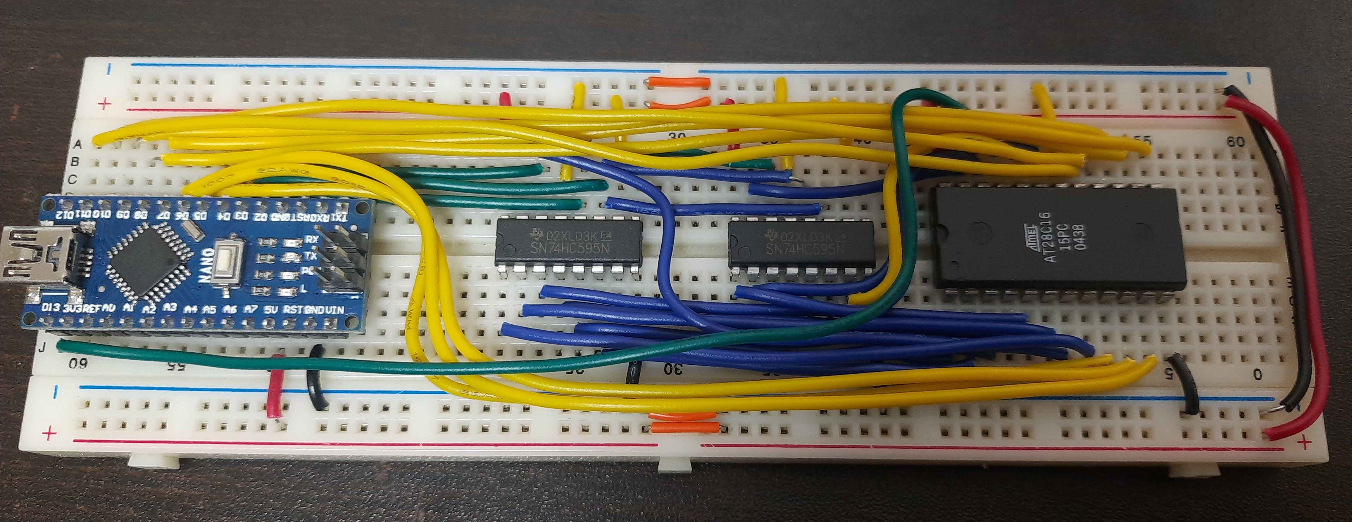
The EEPROM programmer is used to write values to the EEPROM easily using an Arduino. There wasn’t much interesting about building this module. However, it was pretty useful and its Arduino code was easy to understand so modifying it was pretty easy. This module took a total of 2 and a half hrs. At this point, I had posted the Day 7 update on Twitter.
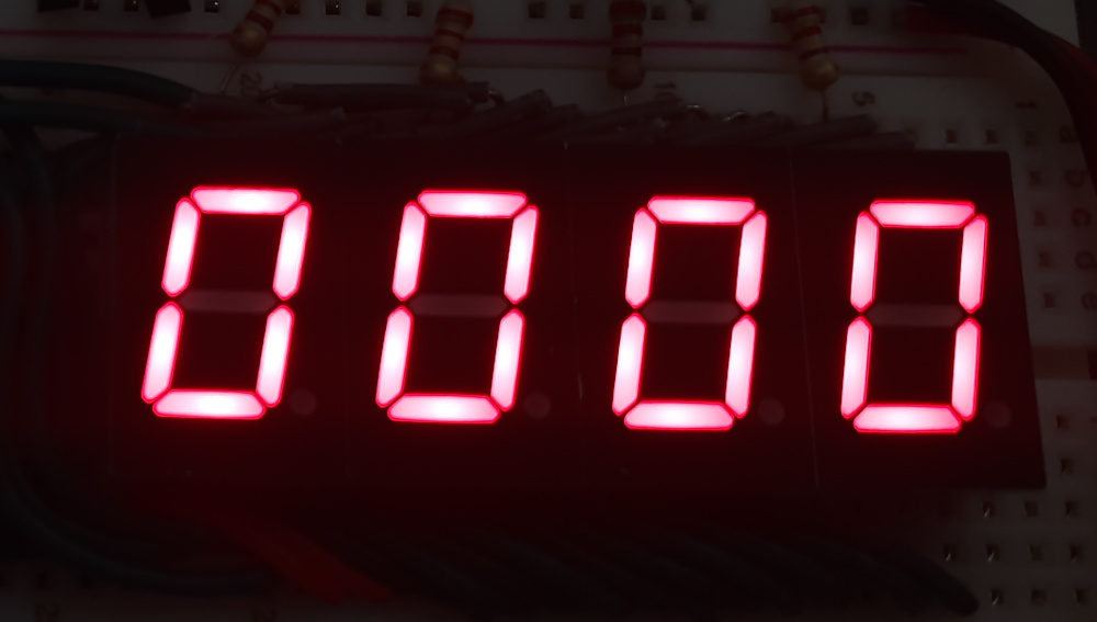
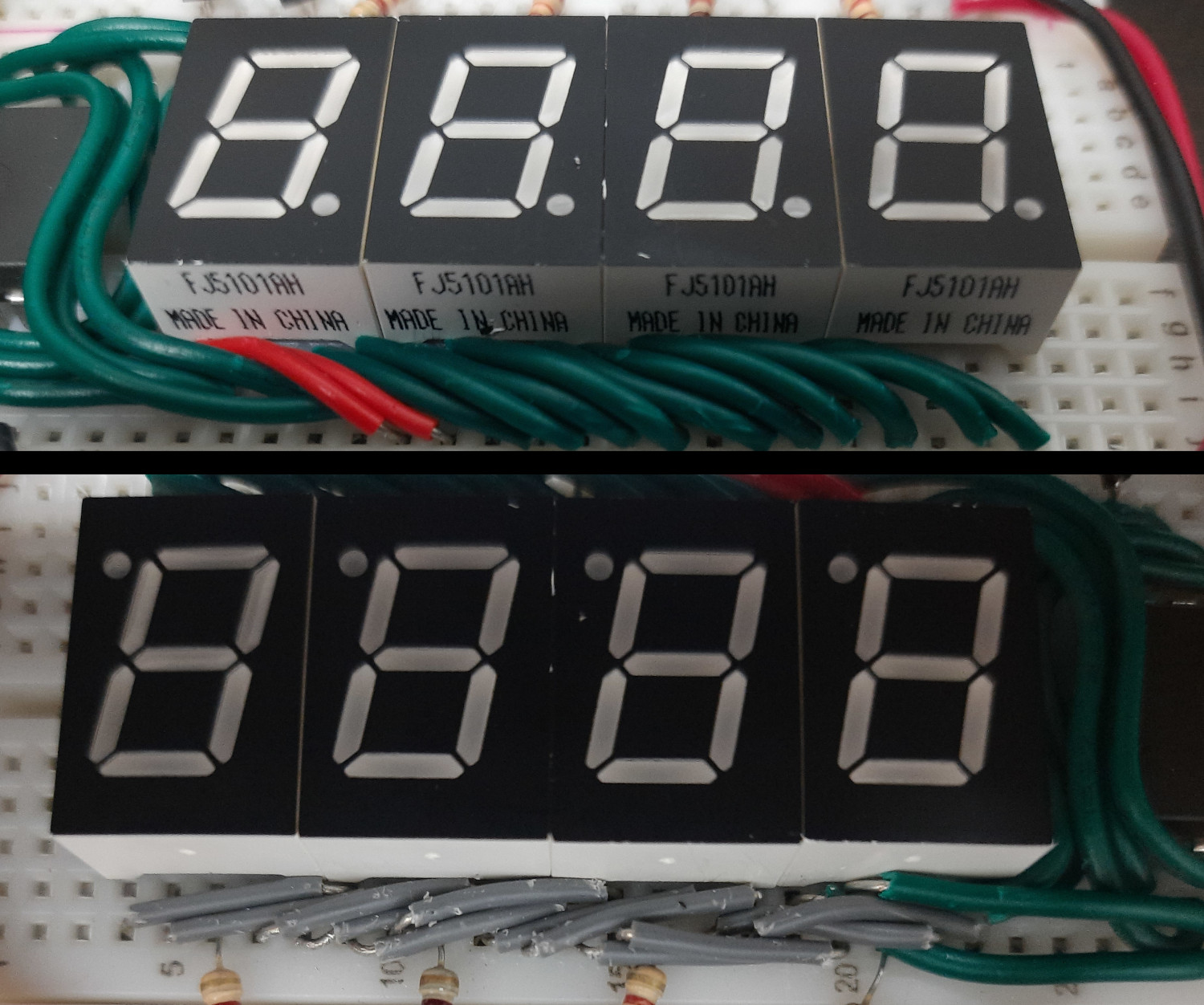
Module 7: The Output Module
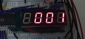
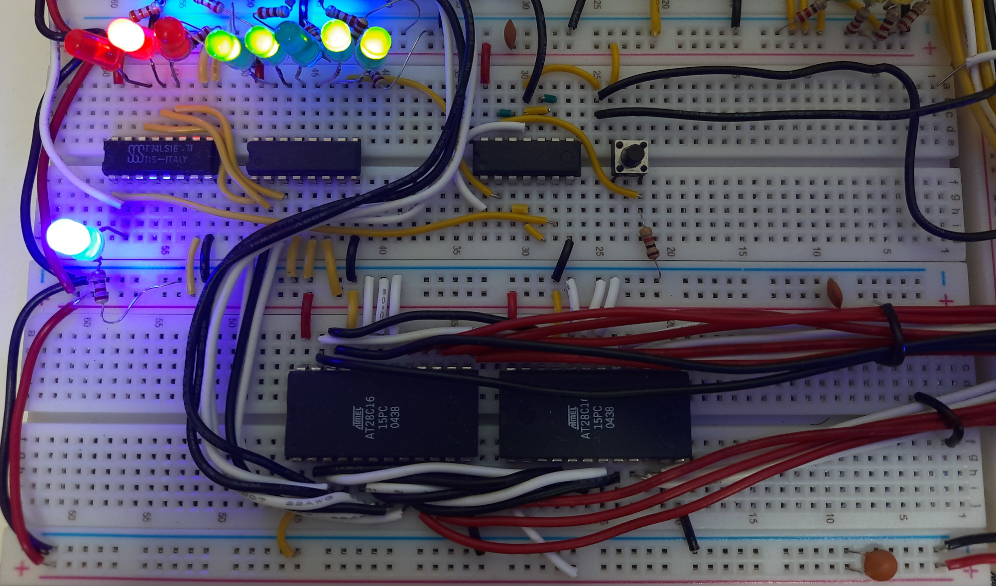
The output module displaying the numbers of the Fibonacci sequence
This module uses an EEPROM to replace the combinational logic to decode the values which are to be used to display numbers on the seven-segment display. Ben has a great video on that topic.
This module uses a separate clock which is used to switch between the 4 seven-segment displays in order to multiplex them and drive them using a single EEPROM instead of 3. The output register is still however connected to the main clock of the system and is synced with the other modules.
I’d also like to mention that the wiring for this module was absolute hell. Remember when I mentioned that the wires were too thick in the first blog post? This is the part where I was barely able to get by and wire them properly. You can even see some of the wires heavily scuffed from how difficult it was to place them.
This module took 4 hours and a half to build. At this point, we had reached Day 8 on Twitter.
Module 8: The Control Logic
This module by far was the hardest and the longest one to build. It took a total of 7 and a half hours, divided as follows:
- The control word and its signals: 2 and a half hours
- CPU microcode and control lines: 4 hours
- The Flags register and all of its connections: 1 hour
When connecting the control word, I connected them in a different order from what Ben did. Using a multimeter, I was able to figure out what was connected where and I modified the code to match what I had connected.
Finally, this module spanned the 2 final updates of Day 9 and Day 10 on Twitter.
Conclusion
The trilogy comes to an end! In this series, we talked about computer architecture, a little bit of electronics, and saw my journey of building The 4043: An 8Bit computer on a breadboard.
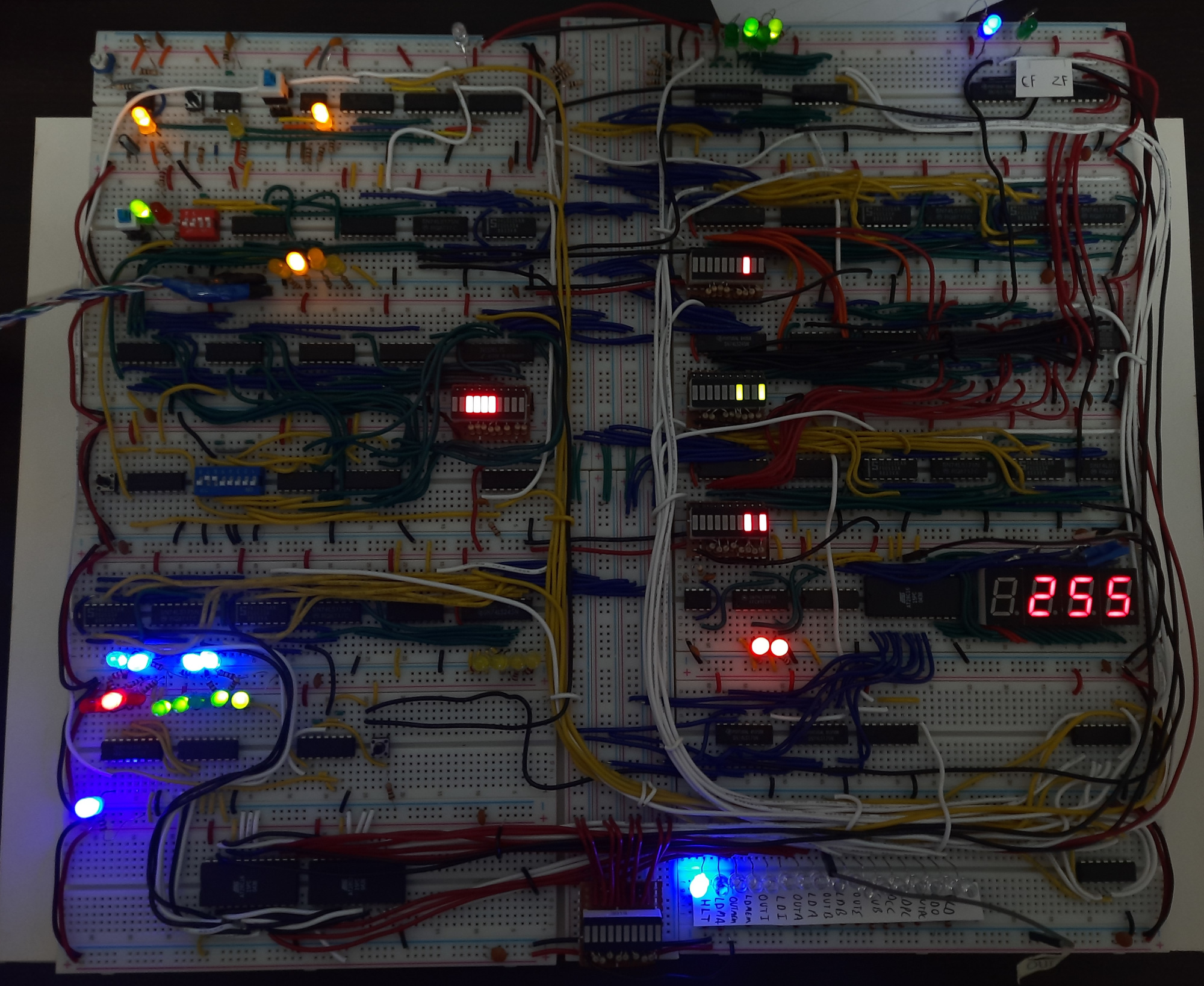
With the project now finished, here is a picture of the finished build.
I also filmed the following video to showcase the whole build and trace the execution while explaining it.
Some Fun Facts
- The computer has 16 bytes of RAM
- The computer draws 800mA from my power supply on idle
- Overall, I used approximately 42 meters of wiring in this build
- The computer in total has 63 chips, including the two shift registers used in the EEPROM programmer
- The build took a total build time of approximately 34 and a half hours. This excludes the time initially spent to research and plan, find chip replacements, and the things I learned the first time I attempted this project
Now What?
Well, for myself, I’ll be taking a bit of a break because this series and the project were a lot of effort. As of writing this exact line, I start connecting the first chip and wire exactly 17 days ago.
As for you, my dear reader, don’t forget to also take a break and drink lots of water :)
You can also possibly check the following:
- Check out the top posts of all time on Ben Eater’s subreddit, where you can find a guy who made his 8Bit computer run the game Snake, or this amazing beautiful build, and a lot of other fun stuff
- Check out the following courses on OpenSecurityTraining, if you want to learn more about modern hardware, assembly, and computer architecture:
- Architecture 1001: x86-64 Assembly - A great primer on x86 assembly and some computer science fundamentals such as boolean logic and other topics needed to get started
- There is Introductory Intel x86: Architecture, Assembly, Applications, & Alliteration - The older version of this course if that’s more your thing
- Architecture 2001: x86-64 OS Internals - An awesome course on x86 architecture. How memory actually works, how the OS uses it, etc… Absolutely outstanding
- There is also Intermediate Intel x86 - The older version of this course if that’s more your thing
- Architecture 1001: x86-64 Assembly - A great primer on x86 assembly and some computer science fundamentals such as boolean logic and other topics needed to get started
- Computer Science Crash Course, which is actually pretty fun and touches on a lot of the topics we discussed here but with many more added topics
- Check out the rest of Ben Eater’s videos, he has a series where he plays with a 6502 processor which is really fun
- If you want to go deeper, you can check out this article, where Ken Shirriff reverse engineers the original Intel 8086 processor’s hardware to show you where its components are
- There are also other blog posts on reverse engineering the microcode for these processors on his blog, which I think is really cool
And that’s it! Thank you so much for reading, I really, really hope you learned something new from this series and from following the updates on Twitter. I hope you enjoyed it.
I’ve worked really hard to prepare and document a lot of this project in advance to be able to write these blog posts. I really hope you enjoyed them and that they taught you something new somehow!
Please share this series with your friends who like adding pointless instructions to their 8Bit CPUs.