In the last post, we talked a bit about computer architecture and how computers generally work. We also got to know a little about how the 8Bit breadboard computer maps to all of that, discussing the clock, registers, and ALU (checked in the image below). I recommend going to read the first part first before continuing to read this post, if you haven’t already.
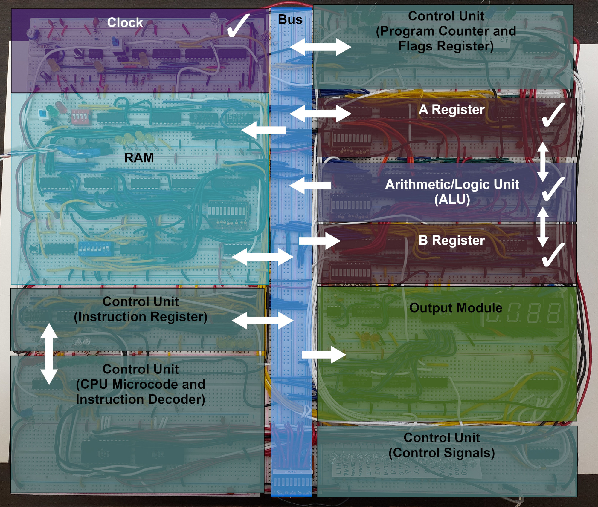
In this post, we’ll talk about the RAM (highlighted in cyan), the bus (highlighted in blue), and one of the parts of the control unit which is the program counter (top left).
Refresher
A quick refresher, we talked last time about the “bare minimum” computer which needs:
- CPU:
- Registers (✓)
- ALU (✓)
- Control Unit (—)
- RAM (—)
- Bus to connect them together (—)
- Clock to sync all of these components together (✓)
Key:
- ✓ - Discussed
- — - Still To be Discussed
By now, we have an idea of how the clock syncs these modules together, how registers are used to store data, and how the ALU operates. Now, we have to ask ourselves: “What really is RAM?” and “What is RAM used for?”.
Random Access Memory
You may be reminded of your favourite Daft Punk album, but bear with me for a moment. Computers generally have two types of memory, volatile and non-volatile. Volatile memory such as RAM loses all of its content upon being powered off. Non-volatile memory such as ROM, NVRAM, and other types we won’t get into stores data in a more permanent way and thus keeps its content after being powered off.
Why use RAM?
Well, you may now be wondering, what is RAM used for? RAM is used to store mainly two things: code and data.
Code
By code here I don’t mean your C or Python lines of code. I mean computer instructions which are stored in binary. As an example, say you write in your C code: x++, which basically increments the x variable by 1.
For simplicity’s sake, let’s assume that the CPU will somehow magically execute this code line using a single instruction. Assuming that you’re using an Intel or AMD modern processor, which both use x86 architecture, we luckily have an instruction for that!
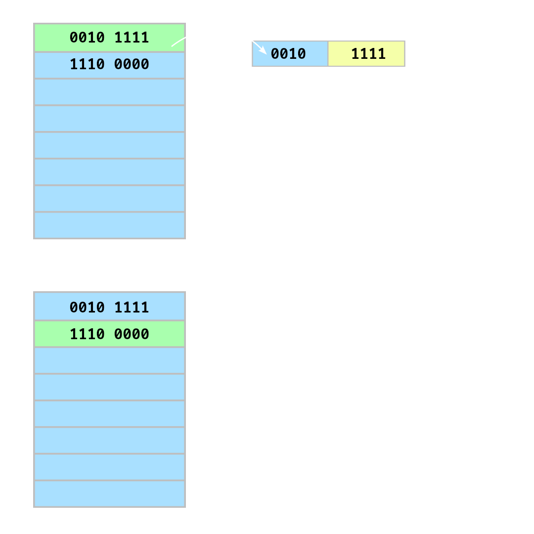
The instruction is inc, which stands for increment and has an opcode of 0x41[1] or 01000001 in binary. This value would then be stored in RAM at some place (address) from which the CPU can read this instruction, decode it, and then execute it. Later, we will look exactly at how these instructions are executed and decoded. For now, let’s just know the fact that they reside in RAM waiting to be fetched by the CPU.
| High Level Code | Assembly | Opcode | Content of RAM |
|---|---|---|---|
x++ |
inc eax |
0x41 |
0100 0001 |
[1] I know that this opcode (0x41) is only for incrementing the eax register, not any inc instruction, please don’t @me. I am trying to simplify things here.
Data
Say you wanted to create a global variable for your program. Where does it get stored? It gets stored in RAM. Specifically, in a data segment. Modern computers divide RAM into segments, but let’s not get into that. The bottom line is that data such as variables and constant values are also stored in RAM, not just program code.
For example, let’s assume you created a global variable: int count. A fixed address (fixed for the duration of the program’s execution) in RAM will be decided by your OS to store the contents of that variable. Depending on the instructions being executed, the CPU may have to access this address in RAM to retrieve this value or to change it.
This may be making you wonder even more, why use volatile memory for all of this? Well, we can possibly achieve the same thing with non-volatile memory. That could be possible, but the main reason we use RAM for this is that it is much, much faster and generally things such as program code and data don’t need any form of long-term persistence. In fact, when a program is executing on your computer, the content of RAM changes so fast that you basically don’t need anything more than very short persistence for its content. As long as the program is still being executed, of course.
Cool, so, so far we got to know that RAM holds our code and data for the CPU to use. But now, we need to answer three questions to get a better picture:
- How does the CPU operate on this code or data?
- How does the CPU know which address in memory to fetch code from?
- How is the code or data moved from RAM to the CPU?
And look no further, we are going to answer them right now!
The Role of Registers
When a CPU wants to operate on data or decode and execute an instruction, it uses registers. For example, if you want to add a value to a variable stored in a memory location, the CPU would first read the value to a register, add to it, and then store it back in memory. Same with code. To decode an instruction, it is loaded from memory into the instruction register. We will get into this in more detail in the next blog post.
Some modern CPUs have ways to directly operate on data in memory without having to move them to registers first. I am really simplifying things here and I don’t want to get into the edge case of each different computer architecture.
Speaking of instruction decoding, how does a CPU know which address in memory to fetch code from?
The Reset Vector
Each CPU is designed to have a reset vector. A reset vector is the default memory location the CPU will start fetching instructions from and executing them. For example, the original Intel 8086 CPU has a reset vector of 0xFFFF0. Our simple breadboard computer has a reset vector of 0 which is the first location in memory.
The CPU then needs a way to go fetch the next instruction after the first one has finished executing.
The Program Counter
A CPU would typically have some sort of counter or a register which stores the address for the command which is to be executed. For x86 processors for example we have the Instruction Pointer (ip/eip/rip) register for 16Bit, 32Bit, and 64Bit respectively.
For our computer, we have a program counter (PC) which can count from 0 to 15, thus being able to address the 16 bytes of memory. Whenever an instruction is decoded, the program counter is incremented by one.
Bonus: Currently we’re executing all instructions sequentially. I want you to try and think of a way to implement a jmp instruction (similar to a goto statement in higher level languages). A jmp instruction basically tells the CPU to execute at a specific address. Have you thought of a way yet? We’ll answer that in the next blog post!
Now that we know how the CPU operates on the code and data. How is it moved into these registers?
The Bus
The bus connects all of these together. If we want to move anything between any of these components we’d have to depend on the bus. A bus in general is just a way of communication between the components. In the case of our breadboard computer, it is a set of 8 connections (wires): one for each bit. Each component has a buffer or a load function which is used to connect and disconnect them from the bus in order to avoid loading unwanted values since it is a single common bus. If the modules aren’t controlled properly, a value could be loaded into the wrong register or stored in the wrong address in memory.
A Single Bus
The von Neumann architecture has only one bus that is used for data and code. So, typically, when you move data between modules, it has to be done in sequential steps and only the relevant components should be enabled to read from the bus or write to it. This is done by the control unit which we will discuss in the next part of this series.
The figure below is an example of how a bus may work. This is a scenario where the user gave the CPU the instruction ADD 0 which adds the value stored at memory address 0 to the A register. We’ll get to assembly in the next blog post, but for now, this description is enough.
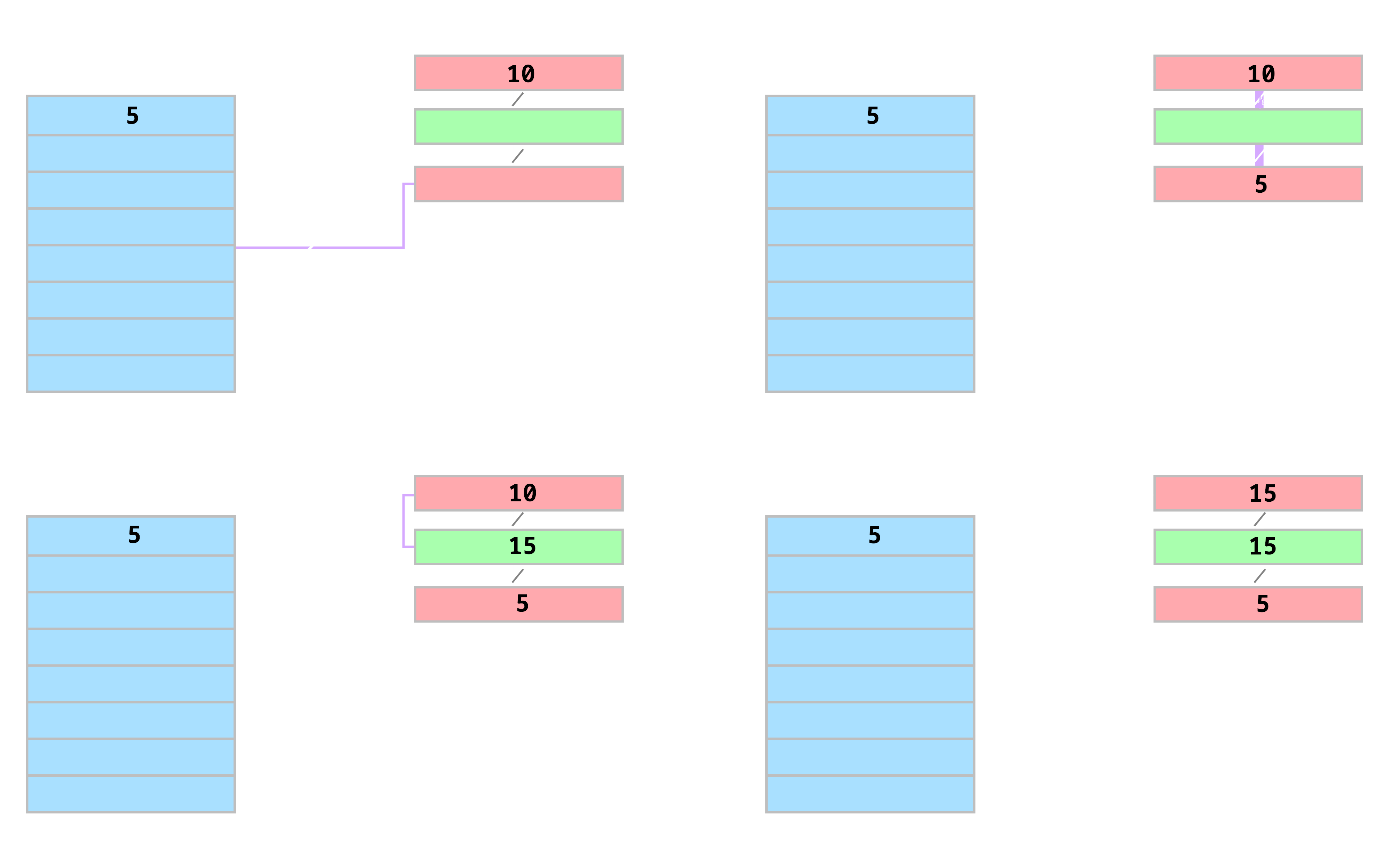
In the figure, we can see the following happen in order:
- The value 5 is copied from address 0 in memory to the B register through the bus
- At this point, register B is loading whatever is on the bus and the memory is outputting the content of address 0 to the bus
- The ALU adds the values of registers A and B which is done without using the bus since the ALU is hard-wired to the A and B registers as we mentioned in the last post
- The ALU is set to output its content to the bus, and the A register is set to read whatever is on the bus. Effectively loading the sum into the A register
- The sum is loaded into the A register and the instruction has now finished execution
This shows how a bus may work in a computer. In fact, this is exactly how our bus works in the 8Bit computer. Let’s now take a look at how all of this is built on the breadboards.
The Build
On days 5, 6, and 7, I built the RAM, the program counter, and started connecting the bus.
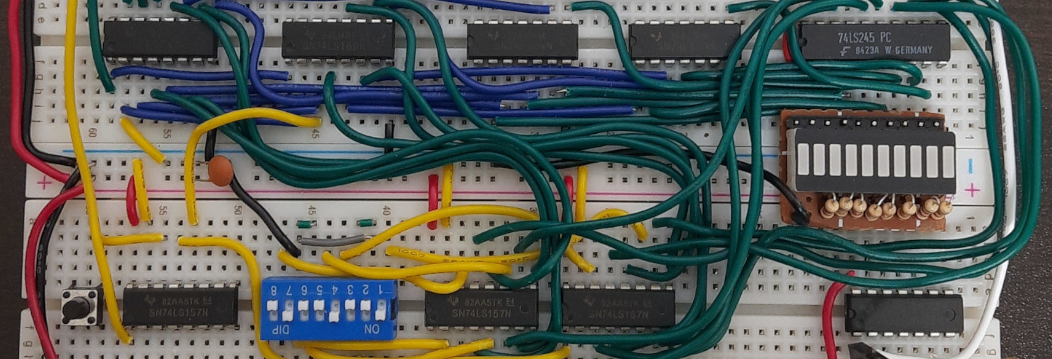
Module 4: The RAM
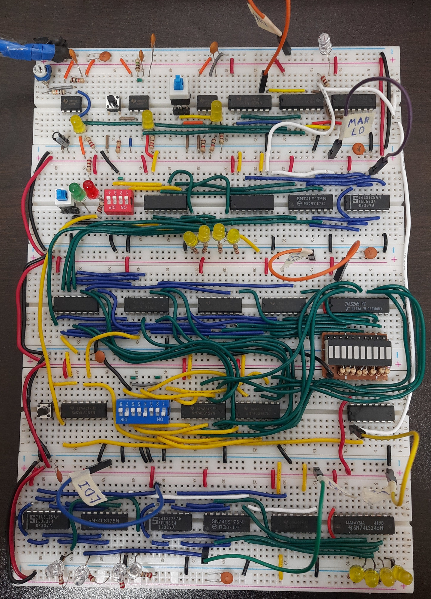
The RAM module (middle 3 boards) with the clock (top) and the instruction register (bottom)
The RAM module consists of three parts:
- The RAM itself, which uses 74LS189 chips. Each chip has 16x4Bit RAM. We use two of these to have a total of 16 bytes
- The memory address register (MAR), which is created the same way as the A and B registers. Except, this time, it is only 4 bits because we only need to address 16 bytes which is addressable by only 4 bits
- The memory data register (MDR), which is used to output data from and write data to memory
Both the data register and the address register have dip switches which we can use to place values in memory at any of the 16 locations. This is used to program the computer later on.
In this module, I didn’t change anything to Ben’s designs except the same replacement I did for the registers (explained in the previous post). One thing I did change is my usual convention of connecting input and outputs to/from chips, I ended up using a different order for the RAM data input bits.
I just chose this order because it made wiring easier, for these specific chips. It is okay to change the order of the bits as long as you’re aware which bit is where and try to keep the wiring consistent across the same module.
This module took a total of 6 and a half hours to build, which are divided as follows:
- RAM: 1 hour and a half
- MAR: 3 hours
- MDR: 2 hours
At this point, I had shared the 5th day’s update on Twitter which was after finishing the RAM module. I had also cleaned up the LED mess using the nice LED bars I mentioned in the previous post.
Module 5: The Program Counter
The program counter was connected exactly like Ben’s. No changes were made at all. However, something important that I have to note is that the first time I attempted this project, I left the clear pin for the 74LS161 chip floating which made it behave very strangely and would often reset itself randomly. This made sense because:
Floating input is the root of all evil.
Before realising it was the clear pin, I thought the chip itself was faulty. This made me test it using an Arduino where I made a clock signal using one of the Arduino’s pins and then read whatever the chip outputted and printed it to the serial monitor. The chip turned out to be fine and I had to check my connections again.
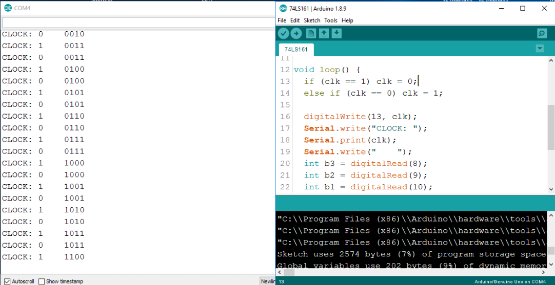
This is generally a very useful technique. Some people on forums and subreddits have even suggested that you should write unit tests for all chips and verify that they’re all working before starting the project. I personally only tested chips when necessary and most of the testing was done manually. I only automated this one because I wanted to remove all other variables and test just the chip itself. I had no extra wires, no bad breadboard connections, nothing. Just the chip being directly powered from the Arduino and having all of its pins connected to it.
By now, the 6th daily update was posted on Twitter. This module took approximately an hour to build.
Connecting the Bus
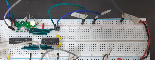
Connecting the bus wasn’t hard at all. However, after connecting it, I realised that a lot of the time the registers would load the values correctly but then the most significant four bits would be always high. I soon realised that this was due to floating inputs to the 74LS245 bus transceiver chips. Connecting these inputs to ground fixed this issue.
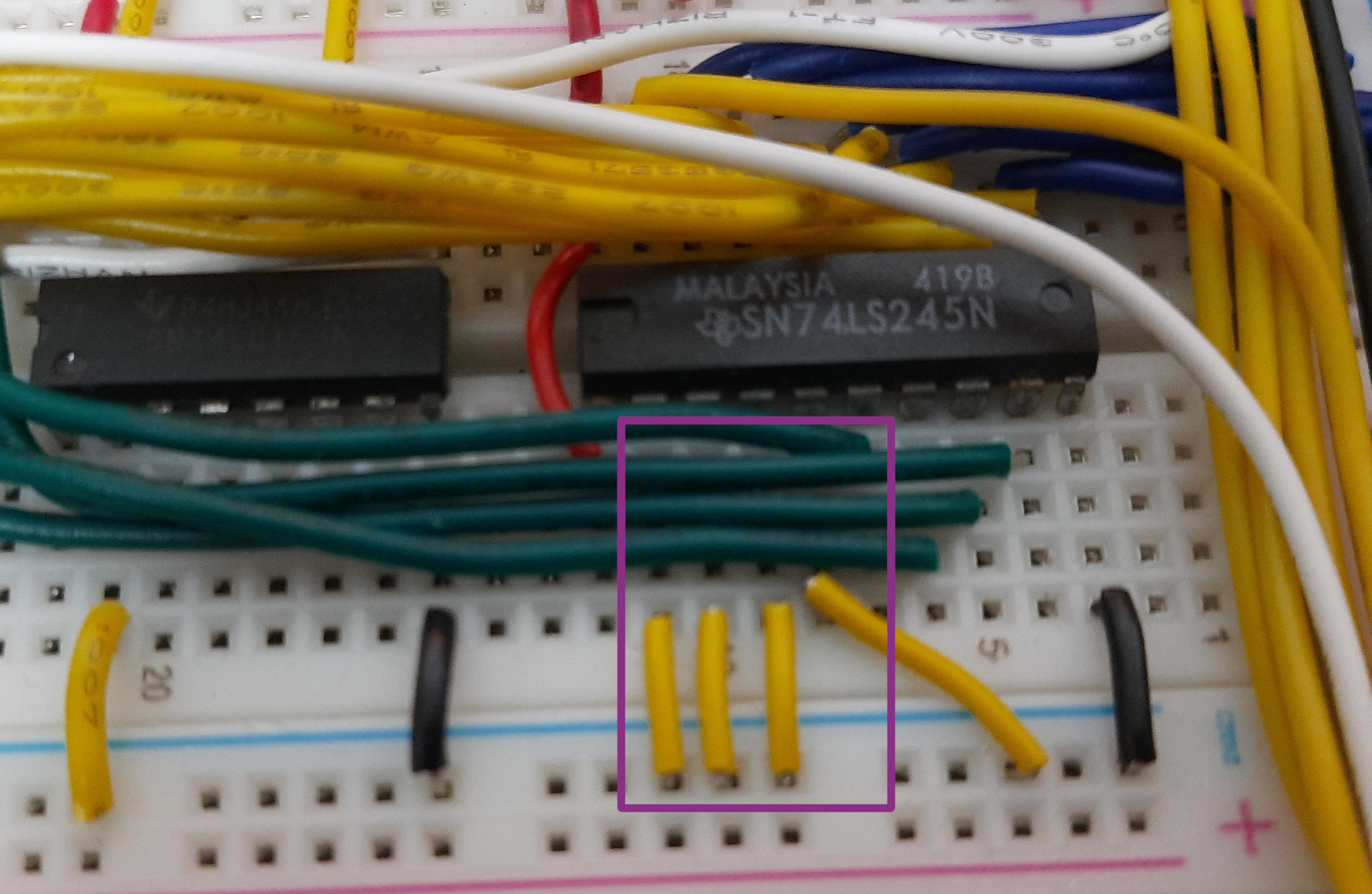
The 74LS245 chips are basically the buffers which have been mentioned before. They’re used to determine if a module will output to the bus or not. On the other hand, LOAD pins on registers and other modules are what allow input in.
Connecting the bus took around an hour. After connecting the bus and finishing the output module (discussed in the next and final blog post), I filmed this video to explain the state of the build so far.
Conclusion
We now have an idea of how code execution works in a computer, how data and code are moved between the modules, and how the computer keeps track of which instruction to execute. But, how does it understand the instructions? How do we program it? I’ll answer these questions in the next post! We will get into how these modules are enabled/disabled according to the instructions and an example of how an output device works.
In the days spanning from the 5th to the 7th, I built the RAM module, the program counter, and started playing around with the bus. The build now has an accumulated build time of 11 and a half plus 8 and a half. Which totalls to 20 hours.
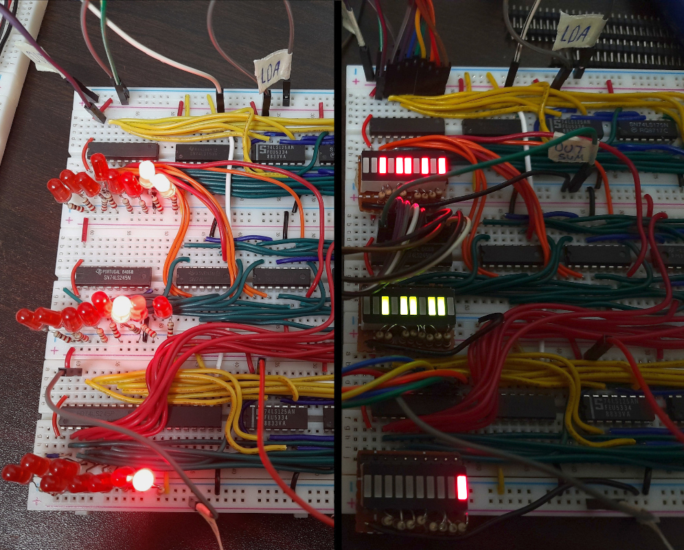
The build looked like this at this stage:
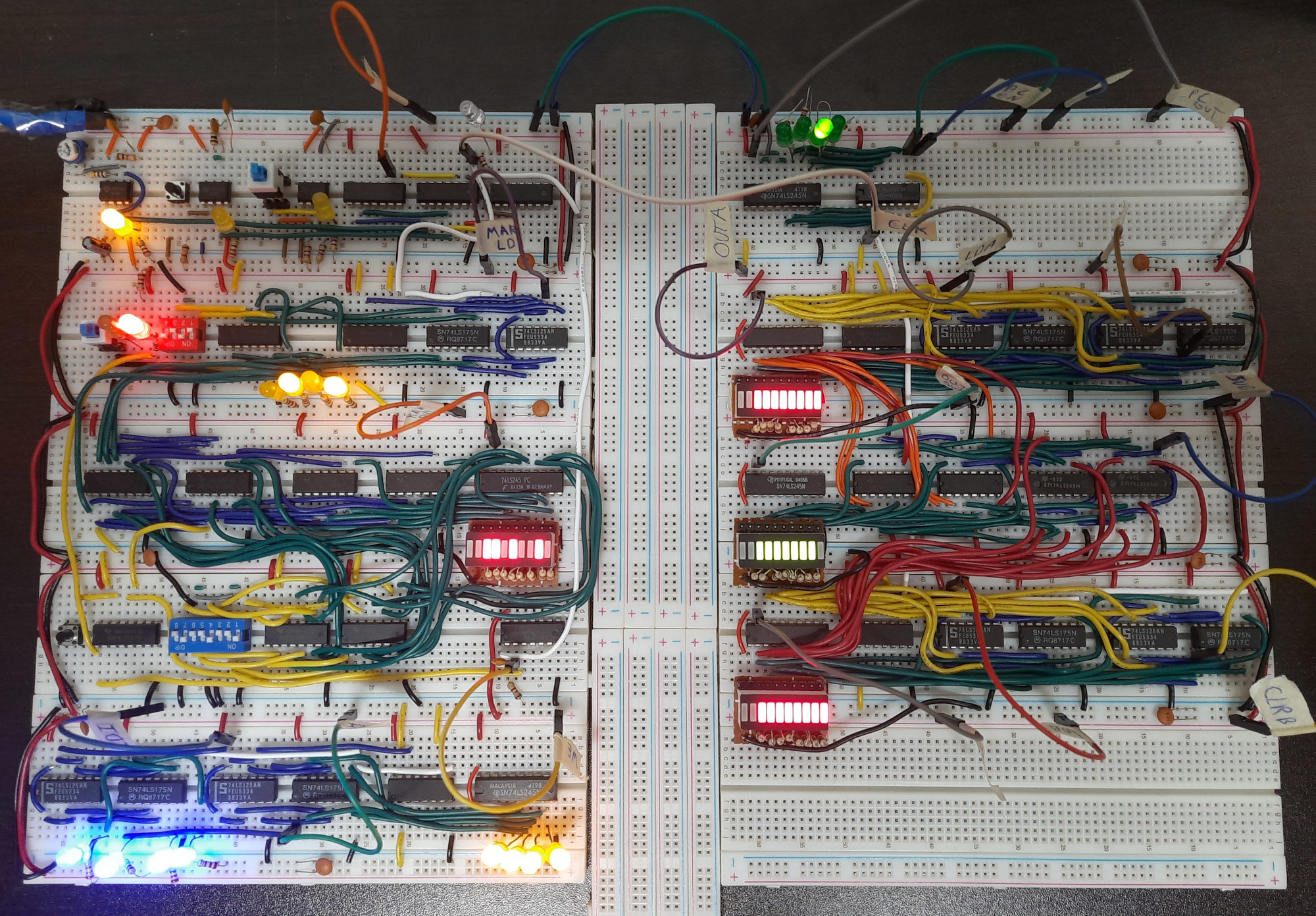
- The ALU is adding 255 to 255 which overflows to 254
- The program counter has counted to 2
- The memory address register is holding the address of value 0101 (5) which was added manually using the dip switches
- Address 5 in memory holds the value 11010010
- The instruction register is holding a value of all 1s
That’s all for now! I hope you enjoyed this post and learned something from it.
Thanks for reading! If you enjoyed this, please share it with your friends that like dereferencing random pointers in memory.