If you’ve been following me on Twitter, you must’ve been seeing some insane dude who is putting some chips on a breadboard and is using a lot of wiring.This may or may not be be giving you college electronics lab PTSD… Anywho, It seems like he’s up to something.
Well, that really isn’t far from what has been happening for the last 2 weeks 😅! For the past few weeks I’ve been building The 4043, an 8Bit Computer inspired by Ben Eater’s. It is a turing complete computer with 2 general purpose registers, a 4-digit seven segment output display, and a whopping 16 bytes of RAM!
Actually, I started this project back in January 2021 but had to delay it for a while. I ended up disassembling it at the start of last year and started over from scratch 2 weeks ago. The only difference is, this time I had a lot more knowledge, better wires, and I had written some documentation last time regarding the mistakes that I made. This made things significantly easier the second time and I’d love to share these tips and experiences with you! Anyway, let’s take it from the start, shall we?
The Beginning
I’ve always wondered how computers work. I mean, I do know assembly and I have a pretty good idea of how operating systems work and how programs execute. I also studied a bit of computer architecture and all that good stuff. However, I still always wondered how computers actually worked. How can all of this “magic” happen through electrical signals of 1s and 0s?
Then I discovered Ben Eater’s channel and quickly started enjoying and learning from every single video on it. I started watching the “Building an 8-bit breadboard computer!” series. Fast forward a few videos and I was motivated to build something similar to the whole thing to actually understand it and have some hands-on experience with it!
So, I headed over to /r/BenEater and read some posts from the community and other people who attempted this project, created a parts list in a spreadsheet, printed it, and headed over to Bab Ellouq in Cairo. The central hub for all electronic components ranging from resistors all the way up to full-blown prototype and development kits and everything in between. 5 hours later, I had most of the parts and the alternatives I needed from different stores. Now it was time to find out, how computers work!
What is in a Computer?
Well, to answer this question, we need to familiarise ourselves with the von Neumann architecture.
The von Neumann Architecture
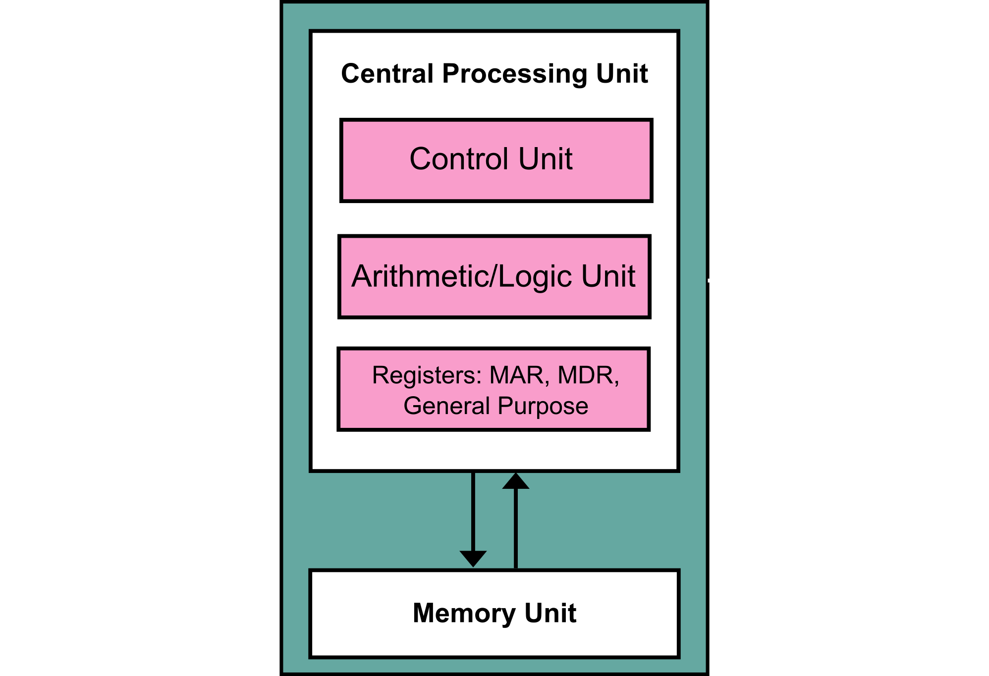
The von Neumann architecture illustrated
The von Neumann architecture is pretty simple. It basically states that the computer at the bare minimum consists of Memory (RAM), a CPU, and a bus that connects them together.
The CPU contains a control unit which decodes instructions and controls the rest of the modules, an ALU which does arithmetic and logic (Subtraction, Addition, ANDing, etc…), and registers which are small storage places used to store data for general purposes and are also used to access memory. These parts work together with input and output devices to perform whatever computations the user wants!
Of course, since our computers need to sync these components together, a clock is used to sync all of these components. What we mean here by a clock isn’t your typical wall clock. A clock in this context is basically just a signal that alternates between high and low (on and off) very frequently so that these modules work in sync. You’d usually see this measured in GHz with modern CPUs, for example, you may find an AMD Ryzen 7 5800X which is a 4.7 GHz CPU. This means that the CPU’s clock oscillates 4.7 billion times per second, generally indicating its speed.

A clock signal example
There are other architectures such as the Harvard architecture but we won’t get into them.
The “Bare Minimum” Computer
So, to summarise - at the bare minimum, a computer needs the following:
- CPU: Registers, ALU, Control Unit
- RAM
- Bus to connect them together
- Clock to sync all of these components together
Logically enough, our 8Bit computer follows this same architecture.
Some Primers
Before we go any further, let’s first clear some basics that will help us throughout the entire project.
Components List
I compiled the list of components I bought and the list of components that ended up making it to the build, in this spreadsheet. I’ve listed them with their prices back when when I bought them. However, I bought these components back in January 2021. So, as you can imagine, the prices have probably changed by now. Fear not, though! My good friend and electronics geek @hegzploit created bgneh which can help you find the cheapest electronic components in a couple of stores. I’ll get to how these components were used and explain more about the alternatives I used for each unavailable component later.
Wiring
The first time I attempted this project, I didn’t find 22 AWG copper wires. I instead bought CAT6 wires. That was genuinely a horrible idea. At first, I blamed the breadboard quality because the wires never stayed in place. However, it turns out the wires are too thin and really aren’t a good fit for breadboards… Or at least for projects this big.
What I’d recommend is getting 22 AWG copper wires or equivalent from electrical supply stores, or buying them from Amazon from another country if you can’t find them at all. Ben recommends the Elenco ones. However, I bought a brand called TUOFENG. The ones I bought were more than fine, but I still found them a little too thick which made wiring in some places very difficult as throughout the project the breadboards keep getting more crowded. I managed just fine, but I am just giving a tip to anyone wanting to attempt this project.
While building the B register, I decided to film this to show how I actually build these modules and wire them. Enjoy!
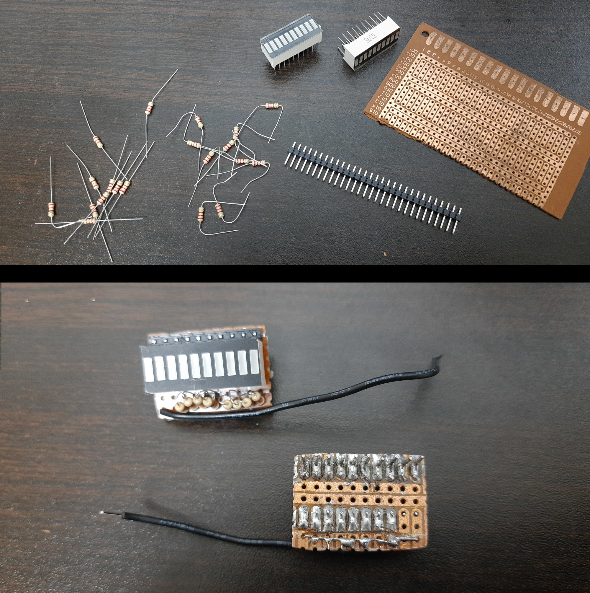
LEDs
Throughout the project, it was absolute hell trying to fit 5mm LEDs where they’re supposed to go. I recommend two of the following options:
- Get 3mm or rectangular LEDs which take up less space
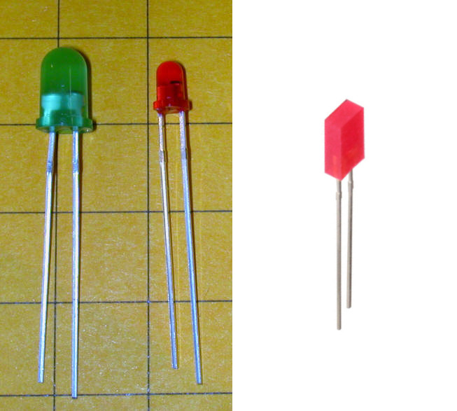
Image credit: trainelectronics.com, electronicaembajadores.com
- Get these nice 10-segment LED bars which don’t cost much at all, but will require some soldering to get them to fit properly
Power
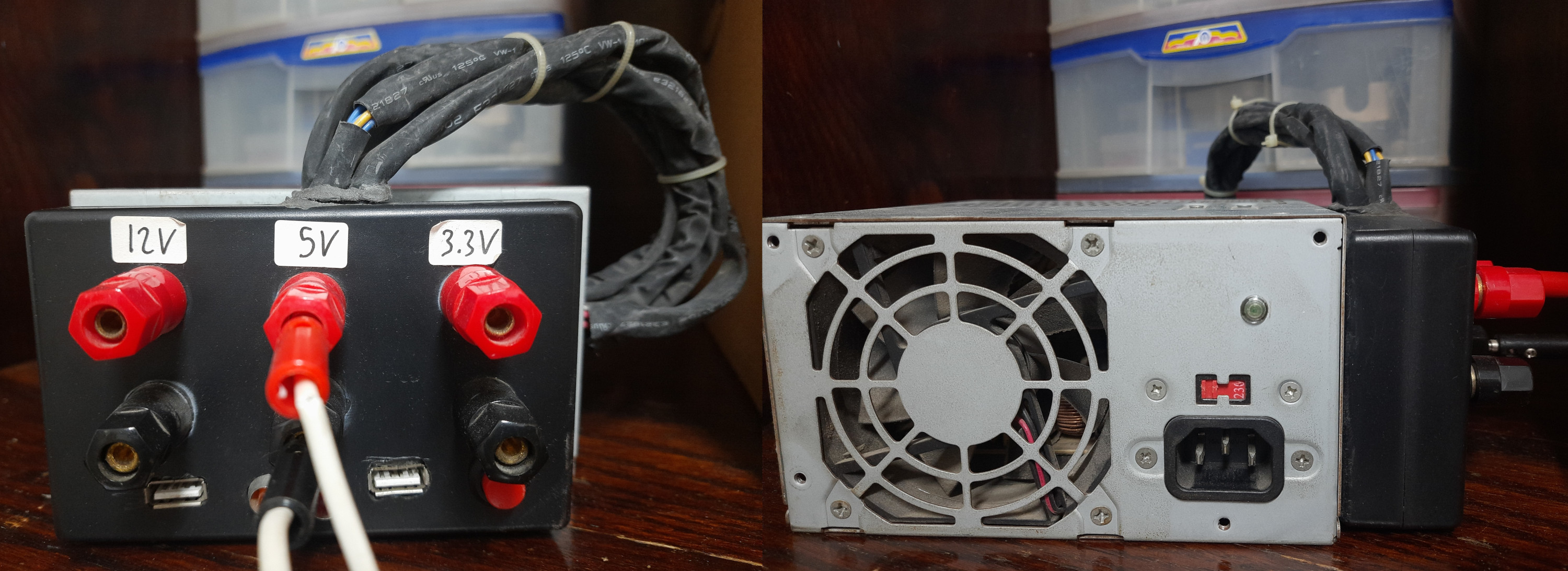
Ben recommends getting a proper power supply that can at least output 1.5-2A. I was personally using my homemade bench power supply which is just an old ATX desktop power supply that I modified. You should also make sure that power is distributed pretty well across the board, you can do so by measuring the voltage at different points in the board far from the power source. The lowest that I was able to get away with before getting into trouble was 3.8V. Your results will vary.
Debugging
To debug pretty much any problem in this project, you’ll need three things:
- A good ol’ Multimeter
- Some LEDs like this array on a breadboard which you can connect to certain points and see which values are high and which are low
- A LOT of patience. Debugging hardware circuits is much more difficult than debugging software
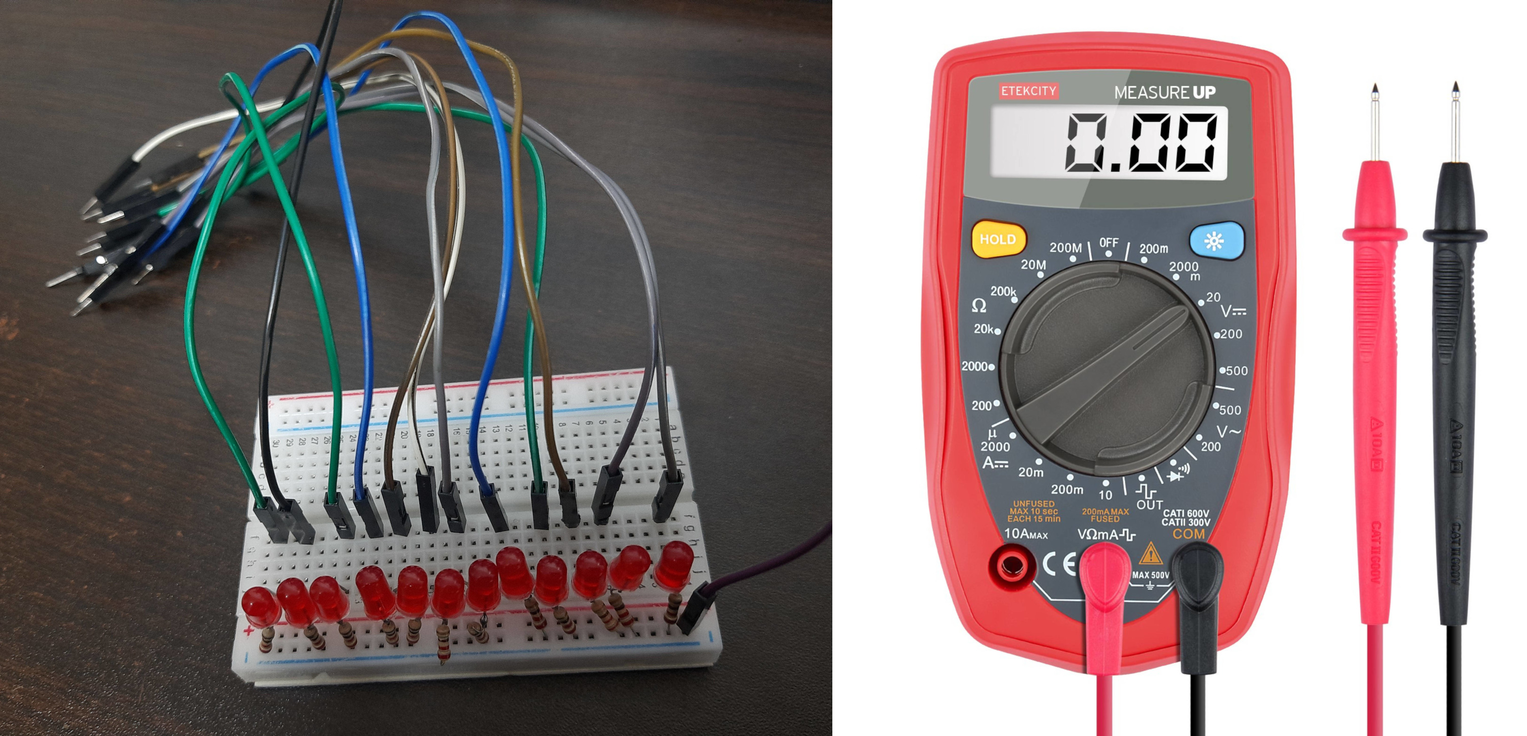
Literally all you need
Community
There is a huge electronics hobbyist community across the whole internet. Whenever you’re stuck with something, look it up and see if anyone has had the same or a similar issue before. Following Ben’s videos exactly doesn’t guarantee that the project will work and you will have to be able to debug your own problems and know how to ask for solutions. Feel free to surf the /r/BenEater subreddit mentioned before. The community there is genuinely amazing and people there have helped me with a couple of things before!
Throughout this series, I won’t get into Ben’s designs or schematics as he can do a much better job at explaining them than I could. I will just explain any alternatives or changes I’ve made to his design.
The Build
On days 1 to 4, I built the clock module, the ALU, and the A and B registers, and the instruction register. For now, let’s focus on the first four (Coloured Purple, Fuchsia, and Red).
Module 1: The Clock Module
The clock module pulsing in auto mode
As I mentioned before, we need a clock signal to be able to sync our modules together. This is a clock module designed by Ben which uses 555 Timer ICs to generate a clock signal. The clock module has two modes: auto, which basically generates a clock signal which a frequency based on the value of a potentiometer and manual mode which allows you to pulse the clock manually, thus single-stepping the computer. You can check out the schematic here.
Cool tip: Get some different capacitor and resistor values to mess around with the 555 timer and get different clock speeds suited to what you want.
The total build time for the module is approximately 2 hours.
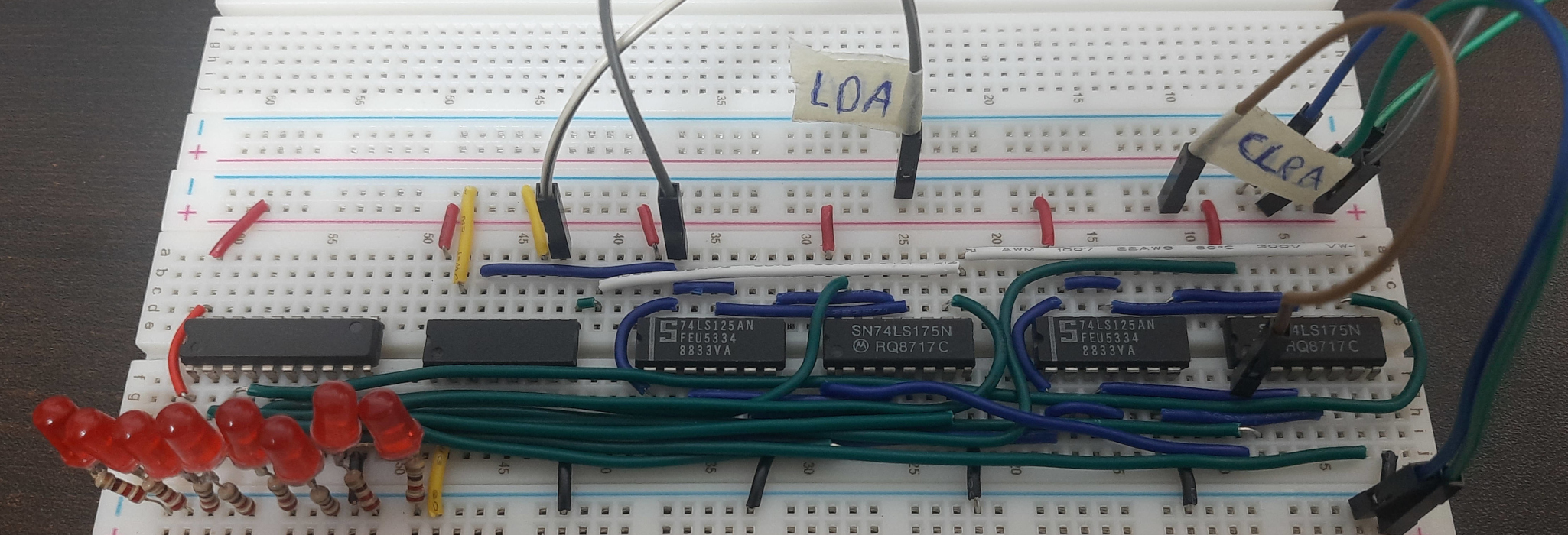
Module 2: The Registers
The registers are part of the CPU and are used to store data which is being operated on at the moment of the execution. Ben uses 74LS173 4Bit D-Type Register chips to make these registers. You can check out the schematics here.
The registers were the first challenge that I had to solve. I faced two problems, the first being the unavailability of the 74LS173 chip, the second issue was that my original workaround was missing something which I’ll get into in a bit. Things will get a bit more technical now, I hope you enjoy it!
Using D Flip-Flops instead of D Registers
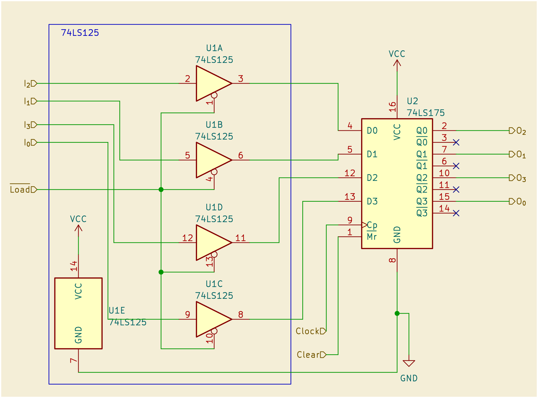
These register chips are essentially D flip-flops but with extra functionality: the load and enable pins. In Ben’s design, the load pins are used to allow a value to be loaded into the registers. After some research and asking around, I was able to figure out that I could use some other chip to isolate the inputs from the D flip-flops until they are given a load signal. A perfect chip for this is a buffer chip. For this specific case, I decided to go for the 74LS125 Quad 3-State buffer chip.
3-State (pronounced tri-state) here means that the output can be either high, low, or disconnected (which is High Impedance mode, often labelled as Z).
The way this is set up is that the 125s act as inputs to the 175s and the Enable pins on the 125s are all connected together to act as an input enable pin which loads the values into the D flip-flops.
Figuring out the Flaw
At first, this seemed to work fine. After testing it more, I realised that the register isn’t holding the value if the clock pulsed when the load signal was high (i.e. not loading). In this case, the register would reset to 0xFF (all 1s).
After checking the truth tables for both of the chips, I figured that I had missed something.
| 74LS175 | 74LS125 | |||||
|---|---|---|---|---|---|---|
| Input | Input | Input | Output | Input | Input | Output |
| CLEAR | CLOCK | D | Q | Load Enable | D | O |
| L | X | X | L | L | L | L |
| H | ↑ | H | H | L | H | H |
| H | ↑ | L | L | H | X | Z |
| H | L | X | Q0 | |||
What was essentially happening is that when the load pin was high, the outputs of the 125 chip would be disconnected from the 175 chip (high impedance mode). This is expected and perfectly normal. The 74LS175 would then behave normally and load the inputs when the clock pulsed, in this case, the inputs defaulted to all 1s because that’s what TTL(74 series) chips default to.
Fixing the Flaw
So even though it seemed like we figured things out and created a load function, what we wanted to actually do was to control the clock for the D flip-flop instead. As without a clock, it wouldn’t load any new values. There were a couple of solutions:
- ANDing the load signal with the clock and then connecting the output of the AND gate to the clock pin on the 175 chip
- This works perfectly and I actually use it later on in the Flags register. Ben also used it in the output register
- Using a multiplexer which selects between ground and the clock depending on the load pin
- This also works really well but adds unnecessary complication
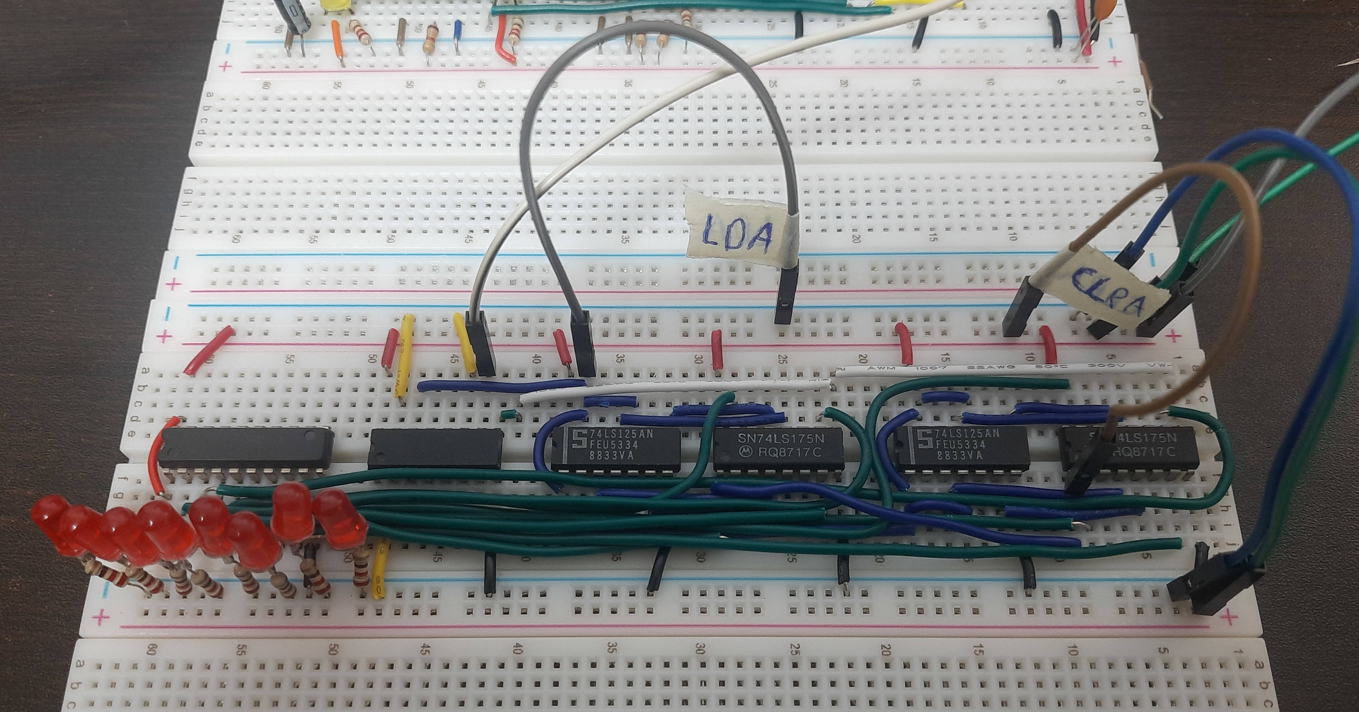
For the A, B, Instruction, and Memory Address registers I went with the second option as I hadn’t thought of the first option yet. And since I had already bought and connected the 74LS125 chips, I kept them connected and just used them as is. I later figured that they were completely unnecessary.
Sigh… Oh well, we live and we learn.
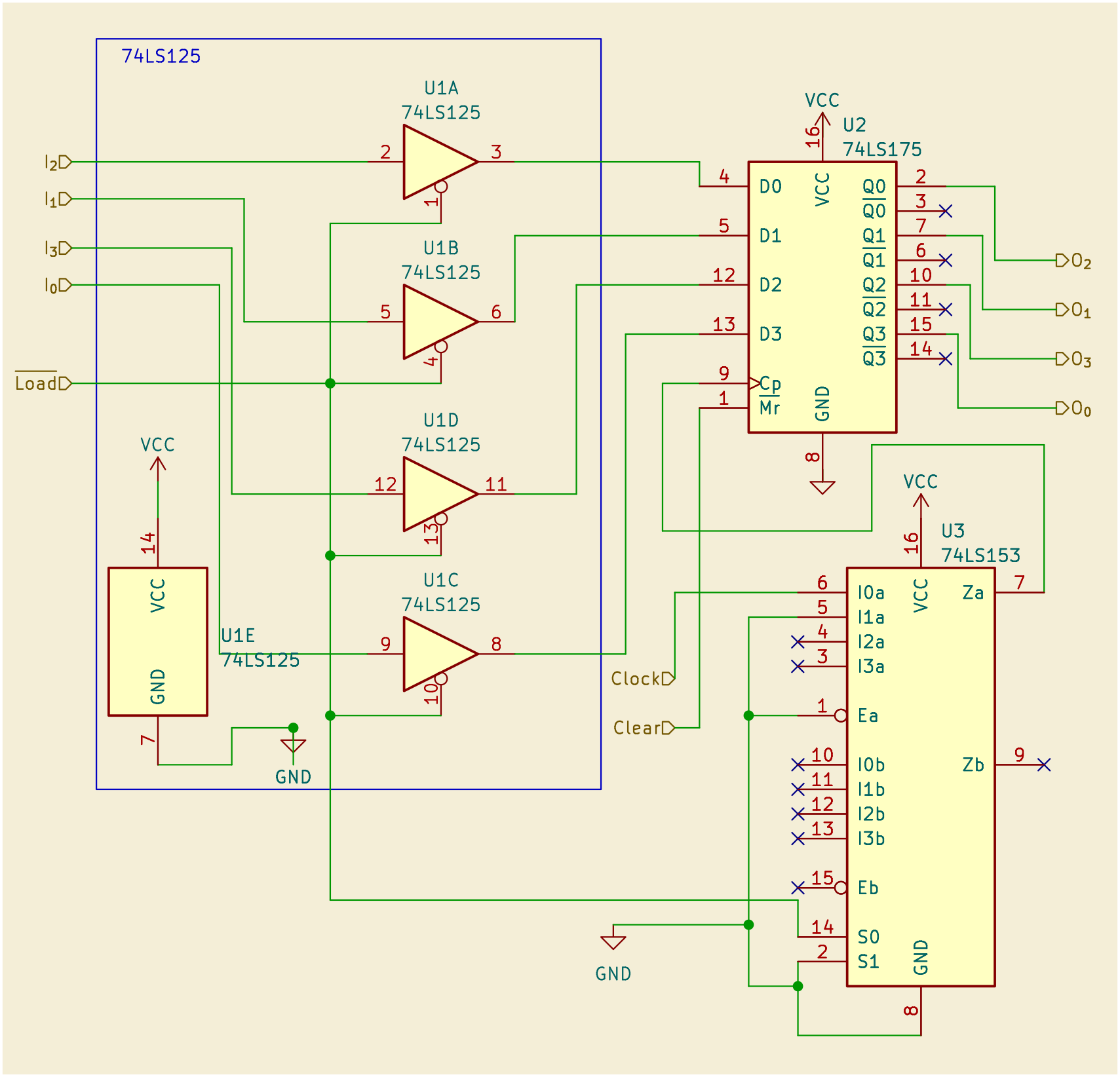
Here is the register’s schematic after connecting the multiplexer. For the multiplexer, I chose the 74LS153 as it was the only mux I found and all I needed was to select between two inputs anyway.
And that was pretty much it! Each register (A, B, and Instruction) took an average of 2 hours to build. At this point I had posted these updates on Twitter: Day 1, Day 2, and Day 3.
Some Nice Tips
- It is nice to label your signal wires using tape or stickers to be able to differentiate them later on
- It may be a good idea to add stickers to your ICs and label their functions, I personally didn’t like doing that. You can try and tell me how it goes!
- When building the Instruction Register, take care of the breadboard orientation so that you don’t have to rewire it again like I did in the first build. Make sure it aligns with the rest of the breadboards and can attach to them.
Module 3: The Arithmetic Logic Unit
The ALU is what gives the computer the ability to perform arithmetic and logic operations. In our case, the ALU uses 4Bit binary adder chips (74LS283) for addition and subtraction. The way subtraction works is that there is a SUB signal which is XORd with each bit going into the adder. This effectively gives us a 1’s complement of the number and then a 1 is added through the carry-in for one of the adders. You can check out Ben’s video which explains this or check out the schematic here. The ALU’s hard wired inputs are the A and B registers.
One tip I found very useful when working with the ALU is to try and keep the inputs and outputs ordered the same across chips as it makes it easier to debug later on if needed and makes the build look cleaner.
The ALU took approximately 3 and a half hours to build. At this point, I had posted the final update which is within the timespan of the 4 days related to this blog post on Twitter: Day 4. I also posted the following video showcasing everything done so far and how it works.
Conclusion
We’ve seen what basic computer architecture is and how The 4043 (our computer here) maps to that.
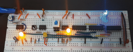
In the first 4 days, I built the clock, the A, B, and Instruction registers, and the ALU. At this point, the build had taken approximately 11 hours and a half. The build looked like this at this stage:
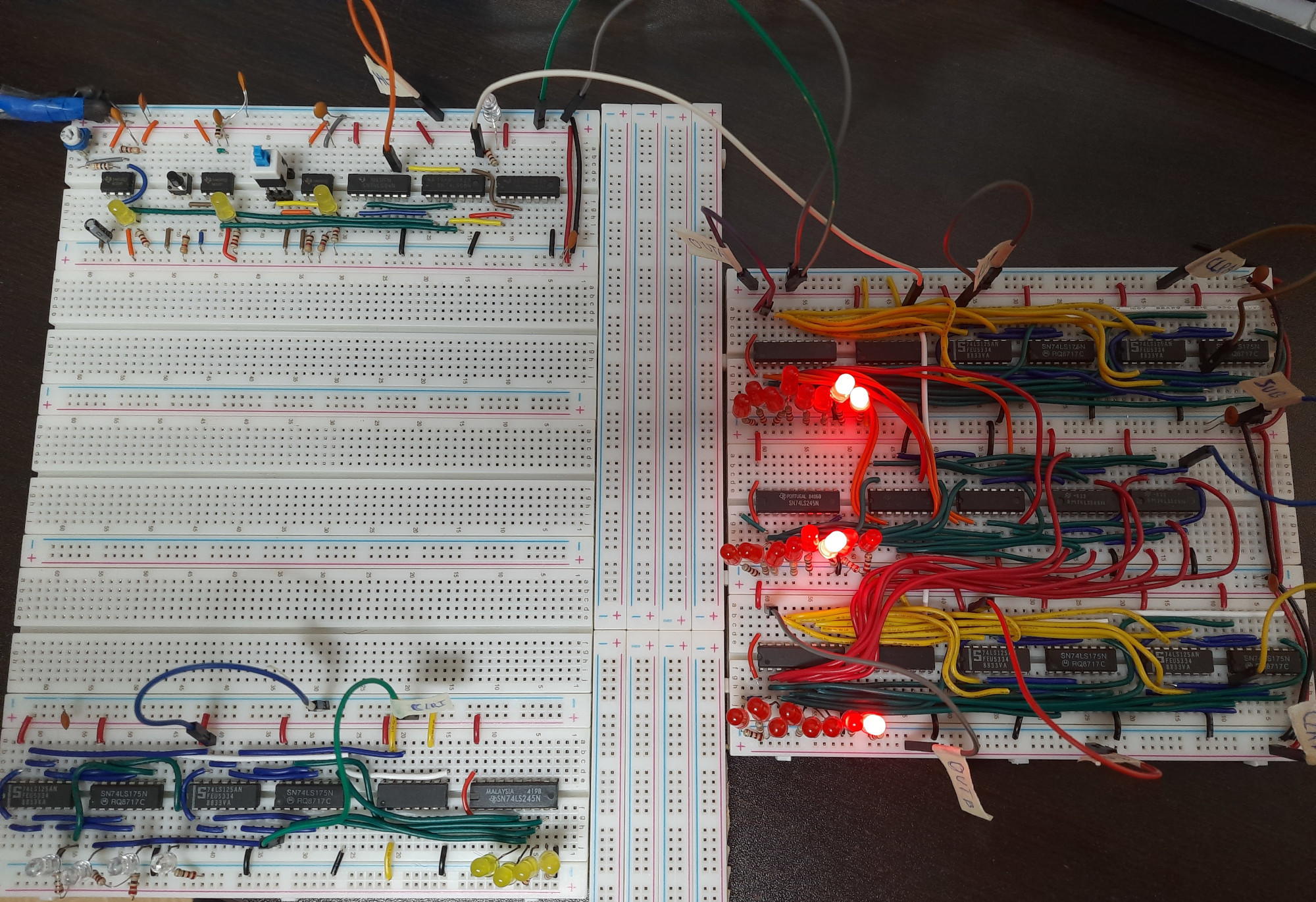
And we can see that the ALU is working. The SUB signal is set low (inactive) and we are adding 0011 (A Register) to 0001 (B Register) which results in (0100) in the ALU’s output(AKA the Sum register).
In the next post, we will take a look at days 5 to 8 which include the RAM, the bus, and the program counter! As always, thanks for reading. I hope you learned something new!
If you enjoyed this post, share it with your friends that love spending 11 hours wiring chips on a breadboard and trying to figure out why an LED won’t turn on.