In a previous blog post, I mentioned that hardware can be reverse-engineered. But, why? And how? Is it legal? We shall embark on a journey today to reverse engineer an Arduino Uno R3 ethically and legally, guiding you through how it is done.
This post is an introduction to hardware reverse engineering. There are many more advanced techniques and ways to reverse engineer boards which I won’t get into this time.
But, wait, isn’t Arduino open-source?
Well, yes. The Arduino Uno R3 is an open-source microcontroller board, but we’ll treat it as a black box. Legally (and I’ll touch on this later), reverse engineering an open-source project is the safest choice for us. We’ll ignore Arduino’s public schematic for now. However, if you decide to give reversing this entire board a try, you can compare your output to the original schematic!
Ethics and Legality of Reverse Engineering
Please be careful. Before doing any type of reverse engineering, make sure it’s ethical and legal to do so where you live. Read the Electronic Frontier Foundation’s Reverse Engineering FAQs for a US perspective on the legality and ethics of reverse engineering. While there is a lot of open-source or public-domain software which you can safely and legally reverse engineer, I can’t say the same about hardware. You can check the list of open-source hardware projects on Wikipedia and maybe you’ll find something you like there.
I am not a lawyer, so don’t take anything I say here as any form of legal advice.
Now that we have our legal bits figured out, let’s get started!
Step 0: Disassembly
This is a prerequisite which we won’t really get into because it isn’t really in our scope. Also, the Arduino board we’re working with doesn’t need disassembly as the board is already exposed.
The only tip I’d give for this stage is to try and find a teardown or disassembly guide for the device you’re trying to reverse engineer, or a similar one.
Step 1: Identifying Components
The first step in reverse engineering hardware is identifying the components on the board.
Chip Markings
Most of the time, there are markings on the chips which are soldered to/placed on the board. These markings usually indicate exactly what a chip is or are some sort of code that you’d have to look up to know what that component is, or what its value is. For example, a chip may have its exact part number on it. A resistor, on the other hand, will usually have either a number on it or colour bands which indicate the resistance value.

An example of how resistor values are read
Identifying the Main Components
“Main” will differ depending on what your goal is with reverse engineering. However, what I mean by “main” here is the parts that stand out and could be quite easy to read the markings on. For example, on this Arduino board, we can see a huge Atmel chip with very clear markings. The chip in this case, especially with the number of pins it has, could be a good place to start.
This isn’t always the case, and the size of the chip doesn’t have anything to do with how important it is. However, as an example, it can just give us a starting point.
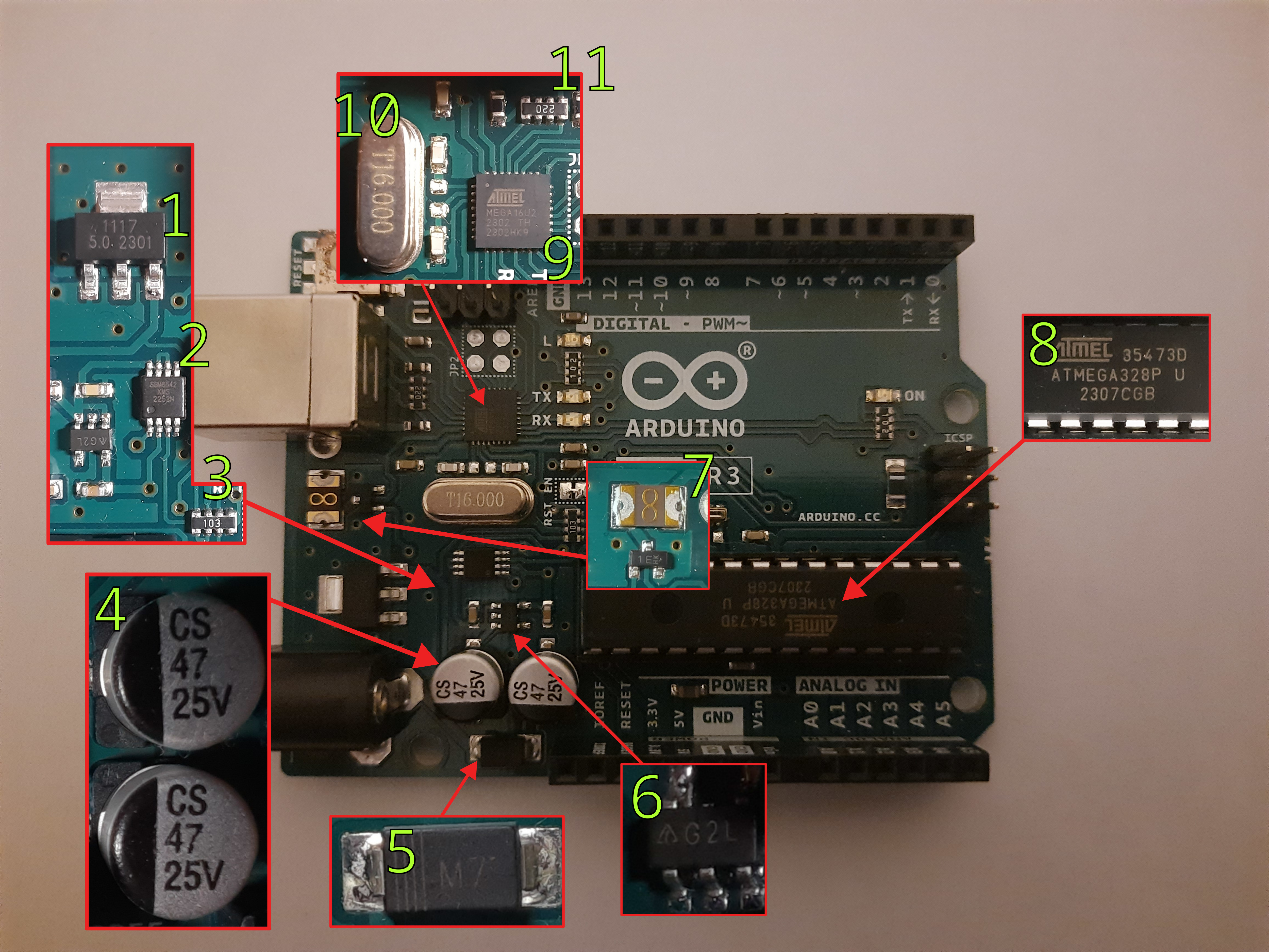
So, let’s do just that! Let’s identify the “main” components.
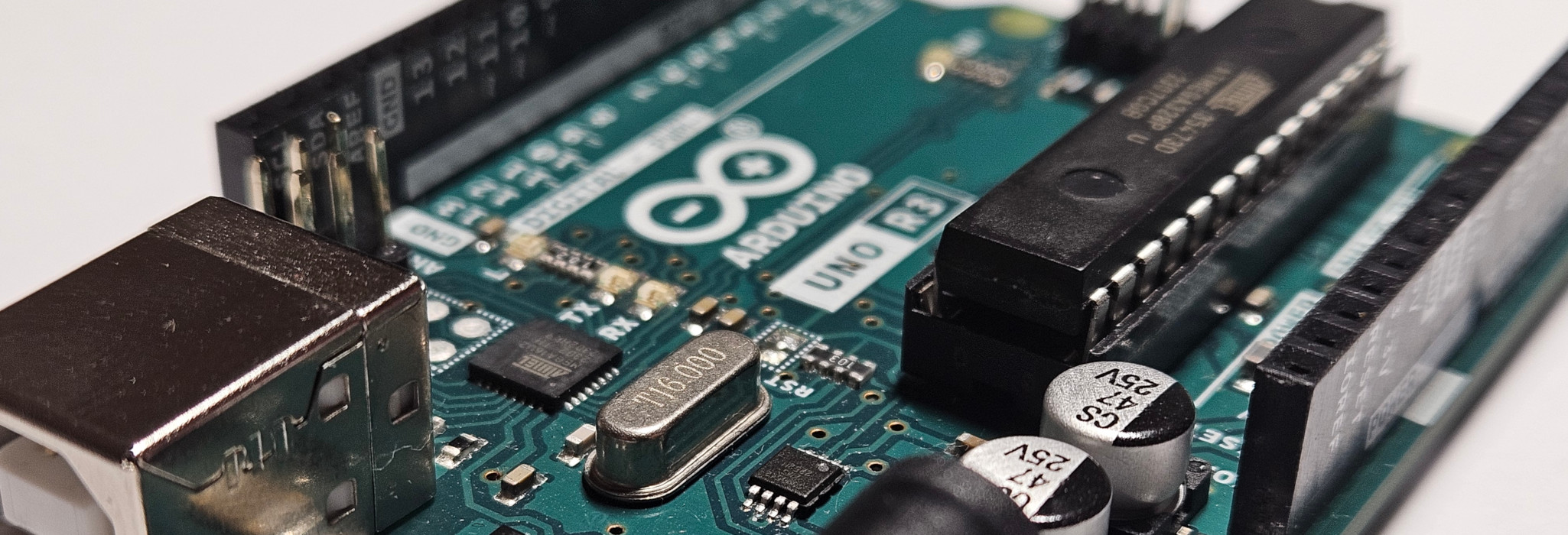
PSA: You may not need a fancy camera, microscope, or high-end phone for this kind of reverse engineering. Depending on your case, you could most likely get by by using the macro lens (or a high zoom in good lighting) on your smartphone. These adequate photos here were taken on an over 3-year-old Samsung Galaxy M31 using the default macro camera mode.
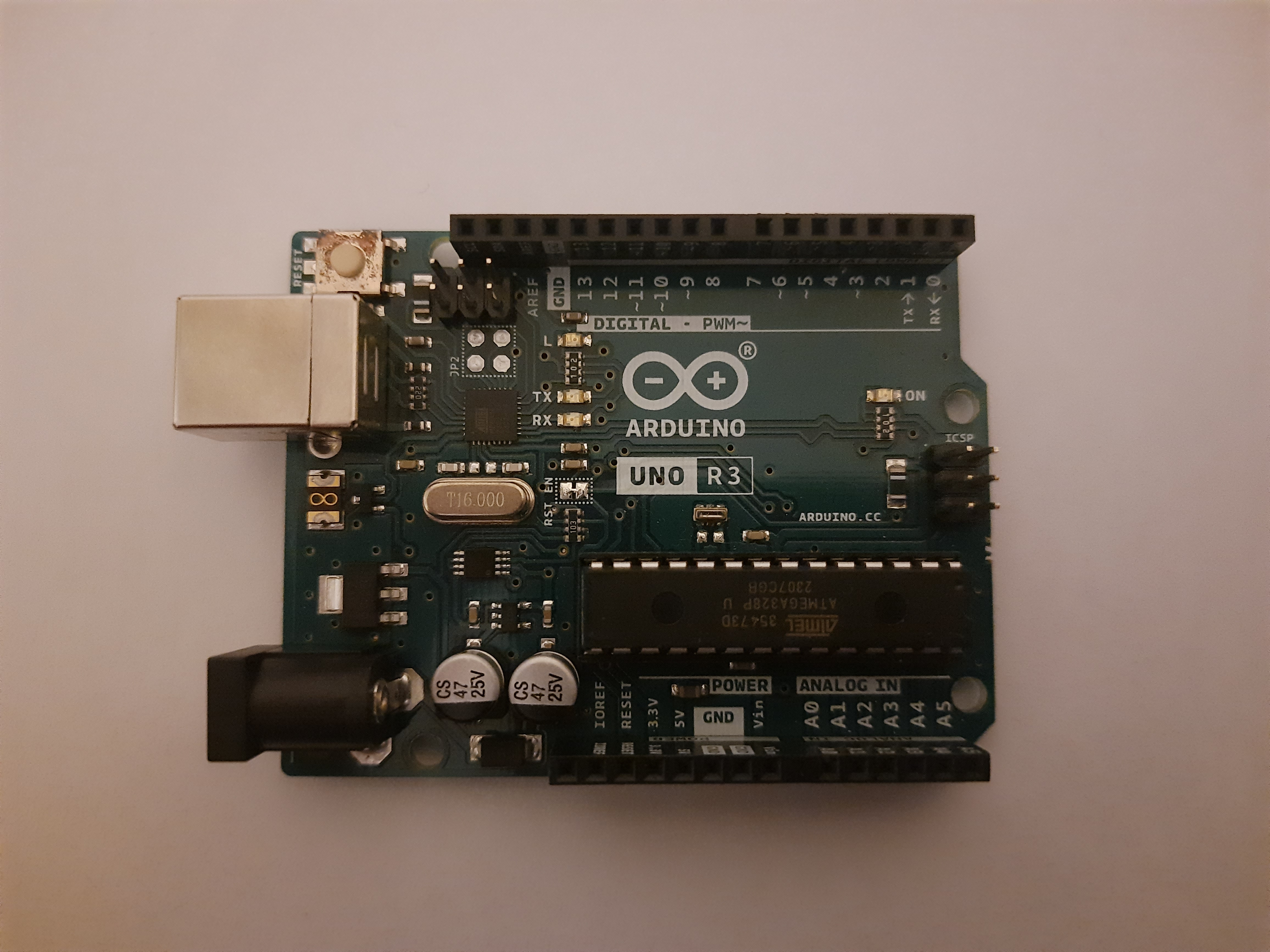
That’s a fair share of components. Where do we begin? It would be a good idea to start with whatever you’re familiar with. But, don’t fret, if you’re not familiar with any of them, let’s get to a search engine!
My First Component
Let’s start with component #1. Assuming that I have no idea what that is, what do I do? Look up whatever is on it. You literally don’t even have to think about it. Just type in whatever you see!

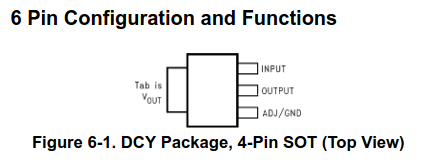
Clicking on the first link takes us to the datasheet of a Low-Dropout Linear Voltage Regulator. Upon inspecting the datasheet, it seems like we have the 5-volt output variant and we can find the pin configuration for it as well.
Congrats! Now we know our first component and what its pins are. We can do the same thing for all of the remaining components to try and identify what they are.
Component List
Following the exact same steps as above, we can identify each component. Right now, it doesn’t matter why each component is in the circuit. All that we care about is that we identify what each component is, which will lead to us understanding what it does, and (hopefully) why it is on this board. Some components are easier than others to identify and find. Let’s take a look at the detective work required! 🕵️
Can I reverse engineer, Daddy?

Component #1 - 1117 Voltage Regulator
This one we already identified. Datasheet here.
Component #2 - SGM8542 Operational Amplifier
A simple search leads to the datasheet here.
Component #4 - 47μF 25V Electrolytic Capacitor
Looking up “CS 47 25V” leads us to this page which tells us that it is, to come as no surprise, a 47μF 25V electrolytic capacitor.
Component #5 - M7 General Purpose Diode/Rectifier
Again, looking up “M7 SMD” leads us to many results which tell us about a series of diodes M1 through M7 with varying reverse voltages. This page has more info on them.
A Surface-Mount Device (SMD) is one that is mounted on the surface of the PCB itself and not through a hole in the PCB. SMDs are usually smaller and allow for a higher component density on the PCB. You’ll know an SMD when you see one!
Component #8 - ATmega328P Microcontroller
The centrepiece of this board. The main microcontroller. Just by looking up the chip marking, we can reach the product page here and from the datasheets, we can find its pin diagram as well.
Component #9 - Atmel MEGA16U2
Just like component #8, we can just look up the chip marking and find ourselves on the product page which contains the summary datasheet. This datasheet tells us that this is a microcontroller with a “USB 2.0 Full-speed Device Module”. The fact that it looks like it is connected to the USB Type-B port suggests that it could be the USB controller.
Please guide me

Component #3 - 10KΩ SMD Resistor Network
Looking up “103 SMD” leads us to some results which look similar. But, not quite exactly. Looking up “103 SMD 8 pins” leads us to learn that this is an SMD resistor network array of 10×103 = 10KΩ.
Component #11 - 22Ω SMD Resistor Network
The same can be done for component #12, which is a 22×100 = 22Ω.
Component #10 - 16MHz Crystal Oscillator
Again, this is much easier if you know what a crystal looks like. Otherwise, you could look up “T16.000” which will eventually lead you to find out that it is a 16MHz crystal oscillator.
Bring ‘em on!

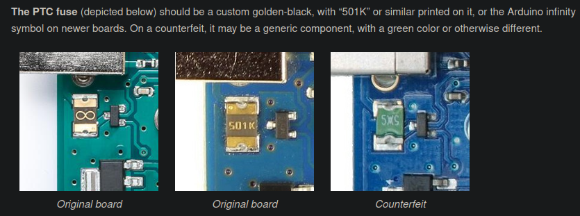
Component #7 - Self-resetting SMD Fuse
This could be hard to search without somewhat knowing what to look for. I know what this is because it is one of the ways to tell if an Arduino is counterfeit or not. According to this article, you can see that they have a custom design for a golden-black SMD fuse. However, most SMD fuses don’t look that different. If you know what an SMD fuse looks like, you’ll probably guess this. If not, then you may be able to figure it out later. Either from the context of the connections or by digging deep enough on the internet.
I am Chips incarnate!

Component #6 - G2L SMD Component
“G2L SMD” leads us to this page, a Chinese online shopping platform, which states that it is a small outline transistor with 5 leads/pins (SOT23-5). This is a little bit misleading, as we can also find this page on Taobao which states that it is a linear voltage regulator in a SOT23-5 package. We could figure that out later at some point. For now, we have sort of an idea of what it is.
Side protip: You can use GIMP, Photoshop, Paint, or any other similar program to label chips and traces
Step 2: Trace, Trace, Trace!
Now that we know what each component is, it is time to figure out how they’re connected. There are multiple techniques you can use to figure this out. Let’s look at some examples.
One of the easy things you can do is trace the connections with your eyes. You will get varying accuracy with this method, depending on how visible the traces are and if the PCB has multiple layers or not. In the image above, we can see that the two labelled pints seem to be connected.
To confirm our connection hypothesis, we can test if the traces are connected with a multimeter. Most multimeters have a continuity test mode, where you can use the leads to test if two points in a circuit are connected.
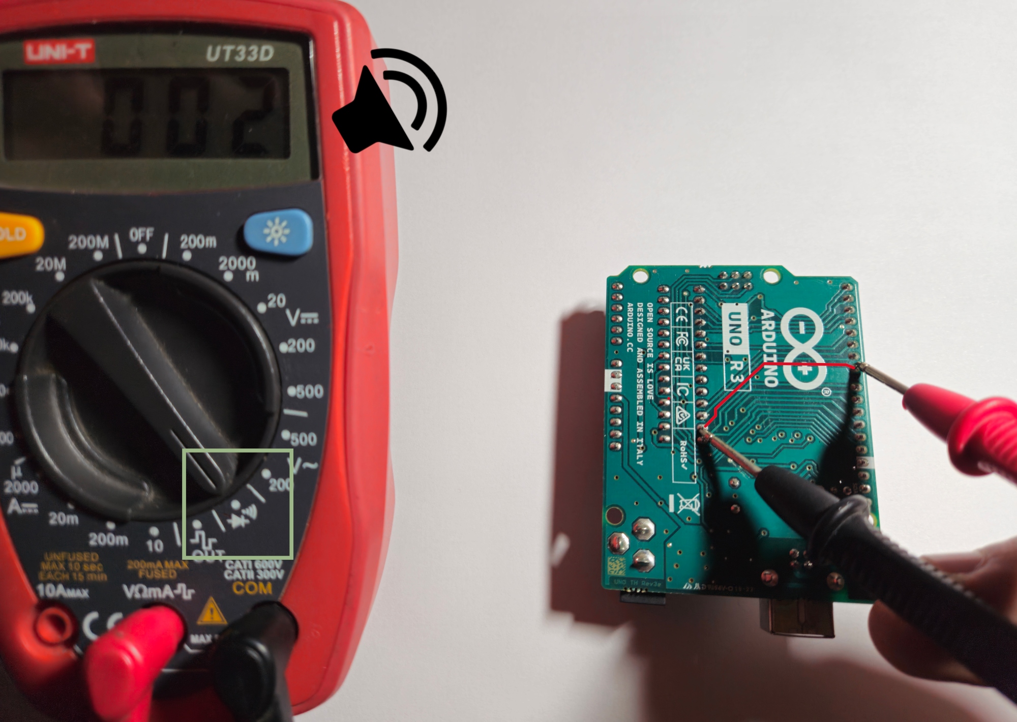
The multimeter is set to test continuity (green box) and the two points are connected (red line)
Indeed, when we test for continuity, we get a buzzing sound from the multimeter which indicates that these two points are connected. What are these, though? Well, these two points are both solder joints. We’d have to flip the board to see which components are soldered at which location. If you’re unsure, just use the multimeter!
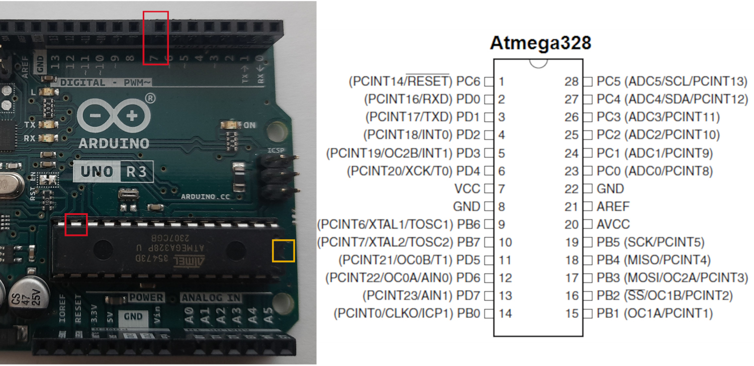
Cross-referencing the datasheet with the pins we found, we can see that pin 13 (PD7) of the ATmega328P is connected directly to the female header labelled “7” which is pin 7 of the Arduino. We can safely assume that the Arduino uses PD7 directly as a digital port. We can tell which way the chip is placed based on the notch (marked in yellow in the picture).
Now all we have to do is do the same for each chip or component on this board, and see where it is connected.
- A) Select a chip or component on the board
- B) Trace where its connections are going
- C) Check the datasheet to see what the functionality or names of the pins are
- This is just to be able to refer to them later as we analyse the circuit a bit further
- D) Rinse and repeat
To keep track of it all, you can use electronic design automation (EDA) software like EasyEDA, KiCad, EAGLE, Proteus, or use pen and paper (the more colourful the better!). Whatever you find easy, can afford, and can obtain legally. Some EDA software is available for students at discounts or even free.
Step 3: Understand (or Guess) the Connections
You can do this step simultaneously with the previous step (i.e. figure out the functionality of each chip on its own, referring to its datasheet), or you can start checking the datasheets after you’ve traced all the connections.
Let’s for example figure out some of the pins of the ATmega328P and what their functions are on this board.
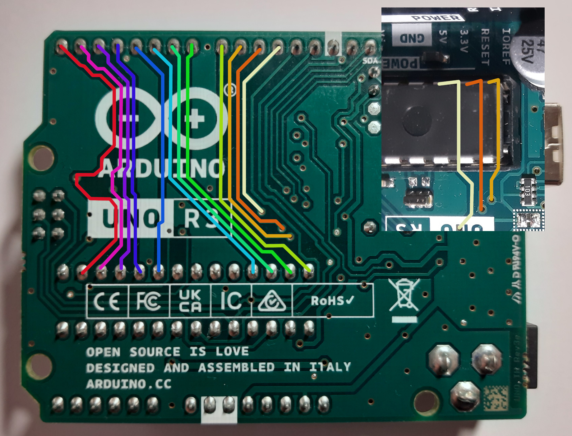
Just by tracing from the pictures we took, we can see that there are some pins on the ATmega chip which are connected to Arduino’s digital pins, just like the previous example. However, when there is a via, the pictures weren’t enough. The yellow, orange, and off-white traces in the picture above are coming out from the Arduino pins into a via. If we flip the board (top right image), we can see the traces coming out of the vias into the ATmega chip. Even though this isn’t really visible to us due to the traces going under components already in place, we can verify it with our trusty multimeter and test to see where the trace coming out of the via goes!
A via is a connection between two or more layers of a PCB. It’s usually a drilled hole and you’ll see a trace on one side terminate at the via and another on the other side start from it (or vice-versa!).
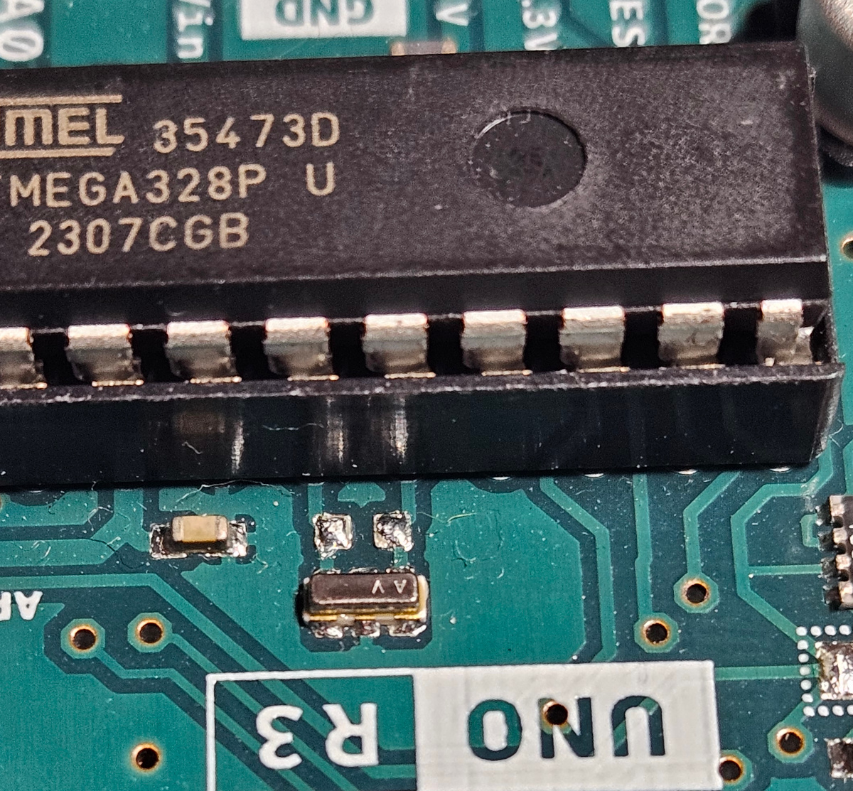
A seemingly small part that stands out is this silver thing connected between two of the ATmega’s pins. We have no idea what that component is and it doesn’t seem to have a very clear marking. However, using our multimeter and by looking at the traces, we can tell that they connect the silver components to pins PB6 and PB7 of the ATmega chip.
To the Datasheet!
Looking at the pinout diagram from the datasheet, we can see that digital pins 0 through 11 (as well as 12 and 13, trust me!) are connected to what seem like I/O ports on the ATmega328P. Arduino pin 0 is connected to ATmega PD0, pin 1 to PD1, pin 2, to PD2, and so on. All the way until pin 8, which is actually connected to PB0, and then pin 9 is connected to PB1, and so on until we reach pin 13 which is connected to PB5.
But, what do these pins on the ATmega actually do? If we check the datasheet, we can find their exact descriptions.
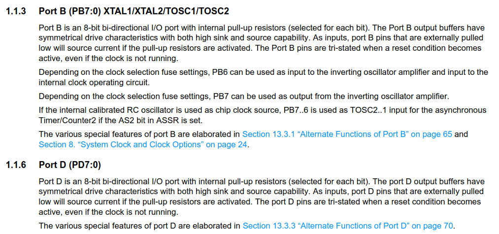
They’re both 8-bit bi-directional I/O ports. Cool! Now we know why they’re connected to Arduino’s digital pins. But, wait a minute… What about PB6 and PB7?
We can see under 1.1.3. Port B - PB6 and PB7 can be connected to a crystal oscillator. We now know what that silver component is :)!
Multi-layer PCBs
Since we mentioned vias, it is worth mentioning that not all boards are double-layer PCBs like this Arduino here. Many boards have way more than two, especially more complex ones. So, “the other side”, can be just a different layer that isn’t the outer one on either side. Depending on the design, you may find only the power traces in the outer layers and all of the data traces in the middle. In that case, it’ll require a bit more work :) For now, we’ll stick to our simple double-layer Arduino board!
Step 4 Onwards
At this point, you can do many things depending on what the goal of reverse engineering the hardware is. There are so many things you can do. It ranges from simply identifying the roles of the chips and drawing the schematic of the board, all the way to analysing what the electronic design of a chip on the board is internally. Let’s take a look at some of the things we can do.
Storage/Flash Dumping and Analysis
If the board has a flash or a form of storage device on it, you could consider dumping it and analysing it. It could have important code, microcode, or anything which could hint at what the hardware is doing or help understand it better.
You can watch this video by Ben Eater on analysing a ROM of an old TV censoring device! Super interesting.
Test Pads or Debug Headers
Some devices make it to the market with test pads or debug headers still connected and enabled on the board. These pads/headers are often used during development or for debugging. However, when they’re left by devs, whether accidentally or on purpose (for debugging or maintenance), they can be a very useful addition to analysis. You can use a logic analyser or an oscilloscope for this and see if you get anything useful. Here’s an example of test pad locations on a Raspberry Pi Zero 2 W, another open-source hardware project.
Decapping and RTL Recovery
Another option to understand chips (especially those which don’t have a datasheet, weren’t documented, or are too old) is to decap them and look at them under a microscope. While that is probably expensive, it can yield some good results. If you don’t want to do it yourself, there are some services online which can do it. An example service is DirtyPCBs’ Dirty Decapping.
I’ve seen some people even X-ray chips and memory and analyse their content after digitally processing the images they got from the X-ray scans.
And then?
With enough time, patience, effort, and takeaway meals, we could reverse engineer the entire board and have an identical schematic for it just like the Arduino’s. However, this post is meant to be an introduction to hardware reverse engineering. Maybe, just maybe, sometime in the future we could do that :). For now, you know that hardware reversing exists and is just as fun as software reverse engineering!
Also, if hardware topics like this make you super curious and interested, you may want to check out The Hardware Hacking Handbook by Colin O’Flynn and Jasper van Woudenberg. Again, just please be careful. Only reverse engineer boards you are legally and ethically allowed to reverse engineer.
Thanks for reading! I hope this blog post was fun to read and was beneficial to you :) If you liked this post, please share it with your friends who take X-rays of flash chips for fun in their spare time!
Partial cover image credit: digital multimeter by Good Father.